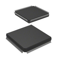
DF2505FC26V Renesas Electronics America, DF2505FC26V Datasheet - Page 823

DF2505FC26V
Manufacturer Part Number
DF2505FC26V
Description
IC H8S/2505 MCU FLASH 144QFP
Manufacturer
Renesas Electronics America
Series
H8® H8S/2500r
Specifications of DF2505FC26V
Core Processor
H8S/2000
Core Size
16-Bit
Speed
26MHz
Connectivity
I²C, SCI
Peripherals
POR, PWM, WDT
Number Of I /o
104
Program Memory Size
384KB (384K x 8)
Program Memory Type
FLASH
Ram Size
32K x 8
Voltage - Supply (vcc/vdd)
3 V ~ 5.5 V
Data Converters
A/D 16x10b; D/A 2x8b
Oscillator Type
Internal
Operating Temperature
-40°C ~ 85°C
Package / Case
144-QFP
Lead Free Status / RoHS Status
Lead free / RoHS Compliant
Eeprom Size
-
- Current page: 823 of 980
- Download datasheet (6Mb)
This LSI has an on-chip clock pulse generator that generates the system clock (φ), the bus master
clock, and internal clocks. The clock pulse generator consists of a system clock oscillator, PLL
(Phase Locked Loop) circuit, clock selection circuit, medium-speed clock divider, bus master
clock selection circuit, subclock oscillator, and waveform generation circuit.
Figure 21.1 shows a block diagram of the clock pulse generator.
Frequency changes are performed by software by settings in the low-power control register
(LPWRCR) and system clock control register (SCKCR).
EXTAL
XTAL
OSC1
OSC2
Legend:
LPWRCR:
SCKCR:
Low-power control register
System clock control register
Subclock
oscillator
oscillator
System
clock
Figure 21.1 Block Diagram of Clock Pulse Generator
Section 21 Clock Pulse Generator
PLL circuit
generation
Waveform
LPWRCR
(×1, ×2)
circuit
WDT_1 count clock
STC0, STC1
φ
SUB
selection
Clock
circuit
System
clock to
φ pin
clock divider
Rev. 6.00 Sep. 24, 2009 Page 775 of 928
Medium-
speed
peripheral modules
Internal clock to
Section 21 Clock Pulse Generator
φ/2 to
φ/32
φ
selection
SCKCR
master
circuit
clock
Bus
REJ09B0099-0600
Bus master clock
to CPU and DTC
SCK2 to SCK0
Related parts for DF2505FC26V
Image
Part Number
Description
Manufacturer
Datasheet
Request
R

Part Number:
Description:
KIT STARTER FOR M16C/29
Manufacturer:
Renesas Electronics America
Datasheet:

Part Number:
Description:
KIT STARTER FOR R8C/2D
Manufacturer:
Renesas Electronics America
Datasheet:

Part Number:
Description:
R0K33062P STARTER KIT
Manufacturer:
Renesas Electronics America
Datasheet:

Part Number:
Description:
KIT STARTER FOR R8C/23 E8A
Manufacturer:
Renesas Electronics America
Datasheet:

Part Number:
Description:
KIT STARTER FOR R8C/25
Manufacturer:
Renesas Electronics America
Datasheet:

Part Number:
Description:
KIT STARTER H8S2456 SHARPE DSPLY
Manufacturer:
Renesas Electronics America
Datasheet:

Part Number:
Description:
KIT STARTER FOR R8C38C
Manufacturer:
Renesas Electronics America
Datasheet:

Part Number:
Description:
KIT STARTER FOR R8C35C
Manufacturer:
Renesas Electronics America
Datasheet:

Part Number:
Description:
KIT STARTER FOR R8CL3AC+LCD APPS
Manufacturer:
Renesas Electronics America
Datasheet:

Part Number:
Description:
KIT STARTER FOR RX610
Manufacturer:
Renesas Electronics America
Datasheet:

Part Number:
Description:
KIT STARTER FOR R32C/118
Manufacturer:
Renesas Electronics America
Datasheet:

Part Number:
Description:
KIT DEV RSK-R8C/26-29
Manufacturer:
Renesas Electronics America
Datasheet:

Part Number:
Description:
KIT STARTER FOR SH7124
Manufacturer:
Renesas Electronics America
Datasheet:

Part Number:
Description:
KIT STARTER FOR H8SX/1622
Manufacturer:
Renesas Electronics America
Datasheet:

Part Number:
Description:
KIT DEV FOR SH7203
Manufacturer:
Renesas Electronics America
Datasheet:


