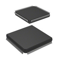
DF2505FC26V Renesas Electronics America, DF2505FC26V Datasheet - Page 439

DF2505FC26V
Manufacturer Part Number
DF2505FC26V
Description
IC H8S/2505 MCU FLASH 144QFP
Manufacturer
Renesas Electronics America
Series
H8® H8S/2500r
Specifications of DF2505FC26V
Core Processor
H8S/2000
Core Size
16-Bit
Speed
26MHz
Connectivity
I²C, SCI
Peripherals
POR, PWM, WDT
Number Of I /o
104
Program Memory Size
384KB (384K x 8)
Program Memory Type
FLASH
Ram Size
32K x 8
Voltage - Supply (vcc/vdd)
3 V ~ 5.5 V
Data Converters
A/D 16x10b; D/A 2x8b
Oscillator Type
Internal
Operating Temperature
-40°C ~ 85°C
Package / Case
144-QFP
Lead Free Status / RoHS Status
Lead free / RoHS Compliant
Eeprom Size
-
- Current page: 439 of 980
- Download datasheet (6Mb)
Writing to RSTCSR: This register must be written to by a word transfer instruction. It cannot be
written to by a byte transfer instruction. Refer to figure 12.7.
The method of writing 0 to the WOVF bit differs from that of writing to the RSTE and RSTS bits.
To write 0 to the WOVF bit, the upper byte must be H'A5 and the lower byte must be H'00. This
clears the WOVF bit to 0 and does not affect the RSTE and RSTS bits.
To write to the RSTE and RSTS bits, the upper byte must be H'5A and the lower byte must be data
to be written to. Bits 6 and 5 in the lower byte are written to the RSTE and RSTS bits,
respectively. This does not affect the WOVF bit.
Reading from TCNT, TCSR and RSTCSR (in the case of WDT_0): These registers are read in
the same way as other registers. The read addresses are allocated in H'FF74 for TCSR, H'FF75 for
TCNT, and H'FF77 for RSTCSR.
Writing 0 to WOVF bit
Writing to RSTE or RSTS bit
Address:
Address:
Figure 12.7 Writing to RSTCSR
H'FF76
H'FF76
15
15
H'A5
H'5A
8 7
8 7
Write data
Rev. 6.00 Sep. 24, 2009 Page 391 of 928
H'00
Section 12 Watchdog Timer (WDT)
0
0
REJ09B0099-0600
Related parts for DF2505FC26V
Image
Part Number
Description
Manufacturer
Datasheet
Request
R

Part Number:
Description:
KIT STARTER FOR M16C/29
Manufacturer:
Renesas Electronics America
Datasheet:

Part Number:
Description:
KIT STARTER FOR R8C/2D
Manufacturer:
Renesas Electronics America
Datasheet:

Part Number:
Description:
R0K33062P STARTER KIT
Manufacturer:
Renesas Electronics America
Datasheet:

Part Number:
Description:
KIT STARTER FOR R8C/23 E8A
Manufacturer:
Renesas Electronics America
Datasheet:

Part Number:
Description:
KIT STARTER FOR R8C/25
Manufacturer:
Renesas Electronics America
Datasheet:

Part Number:
Description:
KIT STARTER H8S2456 SHARPE DSPLY
Manufacturer:
Renesas Electronics America
Datasheet:

Part Number:
Description:
KIT STARTER FOR R8C38C
Manufacturer:
Renesas Electronics America
Datasheet:

Part Number:
Description:
KIT STARTER FOR R8C35C
Manufacturer:
Renesas Electronics America
Datasheet:

Part Number:
Description:
KIT STARTER FOR R8CL3AC+LCD APPS
Manufacturer:
Renesas Electronics America
Datasheet:

Part Number:
Description:
KIT STARTER FOR RX610
Manufacturer:
Renesas Electronics America
Datasheet:

Part Number:
Description:
KIT STARTER FOR R32C/118
Manufacturer:
Renesas Electronics America
Datasheet:

Part Number:
Description:
KIT DEV RSK-R8C/26-29
Manufacturer:
Renesas Electronics America
Datasheet:

Part Number:
Description:
KIT STARTER FOR SH7124
Manufacturer:
Renesas Electronics America
Datasheet:

Part Number:
Description:
KIT STARTER FOR H8SX/1622
Manufacturer:
Renesas Electronics America
Datasheet:

Part Number:
Description:
KIT DEV FOR SH7203
Manufacturer:
Renesas Electronics America
Datasheet:


