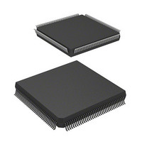
DF2505FC26V Renesas Electronics America, DF2505FC26V Datasheet - Page 519

DF2505FC26V
Manufacturer Part Number
DF2505FC26V
Description
IC H8S/2505 MCU FLASH 144QFP
Manufacturer
Renesas Electronics America
Series
H8® H8S/2500r
Specifications of DF2505FC26V
Core Processor
H8S/2000
Core Size
16-Bit
Speed
26MHz
Connectivity
I²C, SCI
Peripherals
POR, PWM, WDT
Number Of I /o
104
Program Memory Size
384KB (384K x 8)
Program Memory Type
FLASH
Ram Size
32K x 8
Voltage - Supply (vcc/vdd)
3 V ~ 5.5 V
Data Converters
A/D 16x10b; D/A 2x8b
Oscillator Type
Internal
Operating Temperature
-40°C ~ 85°C
Package / Case
144-QFP
Lead Free Status / RoHS Status
Lead free / RoHS Compliant
Eeprom Size
-
- Current page: 519 of 980
- Download datasheet (6Mb)
13.9.7
• Problem in Operation: When DDR and DR are set to 1, SCI clock output is used in clocked
1. End of serial data transmission
2. TE bit = 0
3. C/A bit = 0 ... switchover to port output
4. Occurrence of low-level output (see figure 13.38)
synchronous mode, and the SCK pin is changed to the port pin while transmission is ended,
port output is enabled after low-level output occurs for one half-cycle.
When switching the SCK pin to the port pin by making the following settings while DDR = 1,
DR = 1, C/A = 1, CKE1 = 0, CKE0 = 0, and TE = 1, low-level output occurs for one half-
cycle.
Notes when Switching from SCK Pin to Port Pin
Figure 13.37 Sample Flowchart for Mode Transition during Reception
Read receive data in RDR
Read RDRF flag in SSR
Transition to software
<Start of reception>
standby mode, etc.
standby mode, etc.
Exit from software
operating mode?
Yes
Yes
<Reception>
Initialization
RDRF = 1
Change
RE = 0
No
No
RE = 1
[1]
[2]
[1] Receive data being received
[2] Includes module stop mode
Section 13 Serial Communication Interface (SCI)
becomes invalid.
and watch mode.
Rev. 6.00 Sep. 24, 2009 Page 471 of 928
REJ09B0099-0600
Related parts for DF2505FC26V
Image
Part Number
Description
Manufacturer
Datasheet
Request
R

Part Number:
Description:
KIT STARTER FOR M16C/29
Manufacturer:
Renesas Electronics America
Datasheet:

Part Number:
Description:
KIT STARTER FOR R8C/2D
Manufacturer:
Renesas Electronics America
Datasheet:

Part Number:
Description:
R0K33062P STARTER KIT
Manufacturer:
Renesas Electronics America
Datasheet:

Part Number:
Description:
KIT STARTER FOR R8C/23 E8A
Manufacturer:
Renesas Electronics America
Datasheet:

Part Number:
Description:
KIT STARTER FOR R8C/25
Manufacturer:
Renesas Electronics America
Datasheet:

Part Number:
Description:
KIT STARTER H8S2456 SHARPE DSPLY
Manufacturer:
Renesas Electronics America
Datasheet:

Part Number:
Description:
KIT STARTER FOR R8C38C
Manufacturer:
Renesas Electronics America
Datasheet:

Part Number:
Description:
KIT STARTER FOR R8C35C
Manufacturer:
Renesas Electronics America
Datasheet:

Part Number:
Description:
KIT STARTER FOR R8CL3AC+LCD APPS
Manufacturer:
Renesas Electronics America
Datasheet:

Part Number:
Description:
KIT STARTER FOR RX610
Manufacturer:
Renesas Electronics America
Datasheet:

Part Number:
Description:
KIT STARTER FOR R32C/118
Manufacturer:
Renesas Electronics America
Datasheet:

Part Number:
Description:
KIT DEV RSK-R8C/26-29
Manufacturer:
Renesas Electronics America
Datasheet:

Part Number:
Description:
KIT STARTER FOR SH7124
Manufacturer:
Renesas Electronics America
Datasheet:

Part Number:
Description:
KIT STARTER FOR H8SX/1622
Manufacturer:
Renesas Electronics America
Datasheet:

Part Number:
Description:
KIT DEV FOR SH7203
Manufacturer:
Renesas Electronics America
Datasheet:


