DF2505FC26V Renesas Electronics America, DF2505FC26V Datasheet - Page 725
DF2505FC26V
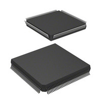
Manufacturer Part Number
DF2505FC26V
Description
IC H8S/2505 MCU FLASH 144QFP
Manufacturer
Renesas Electronics America
Series
H8® H8S/2500r
Specifications of DF2505FC26V
Core Processor
H8S/2000
Core Size
16-Bit
Speed
26MHz
Connectivity
I²C, SCI
Peripherals
POR, PWM, WDT
Number Of I /o
104
Program Memory Size
384KB (384K x 8)
Program Memory Type
FLASH
Ram Size
32K x 8
Voltage - Supply (vcc/vdd)
3 V ~ 5.5 V
Data Converters
A/D 16x10b; D/A 2x8b
Oscillator Type
Internal
Operating Temperature
-40°C ~ 85°C
Package / Case
144-QFP
Lead Free Status / RoHS Status
Lead free / RoHS Compliant
Eeprom Size
-


Table 20.4 Register/Parameter and Target Mode
Notes: 1. The setting is required when programming or erasing user MAT in user boot mode.
20.3.1
The programming/erasing interface registers are as described below. They are all 8-bit registers
that can be accessed in byte. Except for the FLER bit in FCCS, these registers are initialized at a
power-on reset, in hardware standby mode, in software standby mode, or in watch mode. The
FLER bit is not initialized in software standby mode or in watch mode.
Flash Code Control and Status Register (FCCS): FCCS is configured by bits which request the
monitor of error occurrence during programming or erasing flash memory and the download of
on-chip program.
Programming/
Erasing Interface
Register
Programming/
Erasing Interface
Parameter
RAM Emulation
2.
Programming/Erasing Interface Register
The setting may be required according to the combination of initiation mode and read
target MAT.
FCCS
FPCS
FECS
FKEY
FMATS
FTDAR
DPFR
FPFR
FPEFEQ
FUBRA
FMPAR
FMPDR
FEBS
RAMER
Download
⎯
⎯
⎯
⎯
⎯
⎯
⎯
⎯
Initiali-
zation
⎯
⎯
⎯
⎯
⎯
⎯
⎯
⎯
⎯
⎯
⎯
Program
ming
⎯
⎯
⎯
⎯
⎯
⎯
⎯
⎯
⎯
*
1
Rev. 6.00 Sep. 24, 2009 Page 677 of 928
Erasure Read
⎯
⎯
⎯
⎯
⎯
⎯
⎯
⎯
⎯
⎯
*
1
Section 20 Flash Memory
⎯
⎯
⎯
⎯
⎯
⎯
⎯
⎯
⎯
⎯
⎯
⎯
⎯
*
2
REJ09B0099-0600
RAM
Emulation
⎯
⎯
⎯
⎯
⎯
⎯
⎯
⎯
⎯
⎯
⎯
⎯
⎯
Related parts for DF2505FC26V
Image
Part Number
Description
Manufacturer
Datasheet
Request
R

Part Number:
Description:
KIT STARTER FOR M16C/29
Manufacturer:
Renesas Electronics America
Datasheet:

Part Number:
Description:
KIT STARTER FOR R8C/2D
Manufacturer:
Renesas Electronics America
Datasheet:

Part Number:
Description:
R0K33062P STARTER KIT
Manufacturer:
Renesas Electronics America
Datasheet:

Part Number:
Description:
KIT STARTER FOR R8C/23 E8A
Manufacturer:
Renesas Electronics America
Datasheet:

Part Number:
Description:
KIT STARTER FOR R8C/25
Manufacturer:
Renesas Electronics America
Datasheet:

Part Number:
Description:
KIT STARTER H8S2456 SHARPE DSPLY
Manufacturer:
Renesas Electronics America
Datasheet:

Part Number:
Description:
KIT STARTER FOR R8C38C
Manufacturer:
Renesas Electronics America
Datasheet:

Part Number:
Description:
KIT STARTER FOR R8C35C
Manufacturer:
Renesas Electronics America
Datasheet:

Part Number:
Description:
KIT STARTER FOR R8CL3AC+LCD APPS
Manufacturer:
Renesas Electronics America
Datasheet:
Part Number:
Description:
KIT STARTER FOR RX610
Manufacturer:
Renesas Electronics America
Datasheet:

Part Number:
Description:
KIT STARTER FOR R32C/118
Manufacturer:
Renesas Electronics America
Datasheet:

Part Number:
Description:
KIT DEV RSK-R8C/26-29
Manufacturer:
Renesas Electronics America
Datasheet:

Part Number:
Description:
KIT STARTER FOR SH7124
Manufacturer:
Renesas Electronics America
Datasheet:

Part Number:
Description:
KIT STARTER FOR H8SX/1622
Manufacturer:
Renesas Electronics America
Datasheet:

Part Number:
Description:
KIT DEV FOR SH7203
Manufacturer:
Renesas Electronics America
Datasheet: