DF2505FC26V Renesas Electronics America, DF2505FC26V Datasheet - Page 532
DF2505FC26V
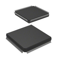
Manufacturer Part Number
DF2505FC26V
Description
IC H8S/2505 MCU FLASH 144QFP
Manufacturer
Renesas Electronics America
Series
H8® H8S/2500r
Specifications of DF2505FC26V
Core Processor
H8S/2000
Core Size
16-Bit
Speed
26MHz
Connectivity
I²C, SCI
Peripherals
POR, PWM, WDT
Number Of I /o
104
Program Memory Size
384KB (384K x 8)
Program Memory Type
FLASH
Ram Size
32K x 8
Voltage - Supply (vcc/vdd)
3 V ~ 5.5 V
Data Converters
A/D 16x10b; D/A 2x8b
Oscillator Type
Internal
Operating Temperature
-40°C ~ 85°C
Package / Case
144-QFP
Lead Free Status / RoHS Status
Lead free / RoHS Compliant
Eeprom Size
-


Section 14 I
Rev. 6.00 Sep. 24, 2009 Page 484 of 928
REJ09B0099-0600
Bit
6
5, 4
3
Bit Name
WAIT
⎯
BCWP
2
C Bus Interface 2 (IIC2)
Initial
Value
0
All 1
1
R/W
R/W
⎯
R/W
Description
Wait Insertion Bit
In master mode with the I
whether to insert a wait after data transfer except the
acknowledge bit. When WAIT is set to 1, after the fall of
the clock for the final data bit, low period is extended for
two transfer clocks. If WAIT is cleared to 0, data and
acknowledge bits are transferred consecutively with no
wait inserted.
The setting of this bit is invalid in slave mode with the I
bus format or with the clocked synchronous serial format.
Reserved
These bits are always read as 1, and cannot be modified.
BC Write Protect
This bit controls the BC2 to BC0 modifications. When
modifying BC2 to BC0, this bit should be cleared to 0 and
use the MOV instruction. In clock synchronous serial
mode, BC should not be modified.
0: When writing, values of BC2 to BC0 are set.
1: When reading, 1 is always read.
When writing, settings of BC2 to BC0 are invalid.
2
C bus format, this bit selects
2
C
Related parts for DF2505FC26V
Image
Part Number
Description
Manufacturer
Datasheet
Request
R

Part Number:
Description:
KIT STARTER FOR M16C/29
Manufacturer:
Renesas Electronics America
Datasheet:

Part Number:
Description:
KIT STARTER FOR R8C/2D
Manufacturer:
Renesas Electronics America
Datasheet:

Part Number:
Description:
R0K33062P STARTER KIT
Manufacturer:
Renesas Electronics America
Datasheet:

Part Number:
Description:
KIT STARTER FOR R8C/23 E8A
Manufacturer:
Renesas Electronics America
Datasheet:

Part Number:
Description:
KIT STARTER FOR R8C/25
Manufacturer:
Renesas Electronics America
Datasheet:

Part Number:
Description:
KIT STARTER H8S2456 SHARPE DSPLY
Manufacturer:
Renesas Electronics America
Datasheet:

Part Number:
Description:
KIT STARTER FOR R8C38C
Manufacturer:
Renesas Electronics America
Datasheet:

Part Number:
Description:
KIT STARTER FOR R8C35C
Manufacturer:
Renesas Electronics America
Datasheet:

Part Number:
Description:
KIT STARTER FOR R8CL3AC+LCD APPS
Manufacturer:
Renesas Electronics America
Datasheet:
Part Number:
Description:
KIT STARTER FOR RX610
Manufacturer:
Renesas Electronics America
Datasheet:

Part Number:
Description:
KIT STARTER FOR R32C/118
Manufacturer:
Renesas Electronics America
Datasheet:

Part Number:
Description:
KIT DEV RSK-R8C/26-29
Manufacturer:
Renesas Electronics America
Datasheet:

Part Number:
Description:
KIT STARTER FOR SH7124
Manufacturer:
Renesas Electronics America
Datasheet:

Part Number:
Description:
KIT STARTER FOR H8SX/1622
Manufacturer:
Renesas Electronics America
Datasheet:

Part Number:
Description:
KIT DEV FOR SH7203
Manufacturer:
Renesas Electronics America
Datasheet: