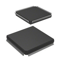
DF2505FC26V Renesas Electronics America, DF2505FC26V Datasheet - Page 756

DF2505FC26V
Manufacturer Part Number
DF2505FC26V
Description
IC H8S/2505 MCU FLASH 144QFP
Manufacturer
Renesas Electronics America
Series
H8® H8S/2500r
Specifications of DF2505FC26V
Core Processor
H8S/2000
Core Size
16-Bit
Speed
26MHz
Connectivity
I²C, SCI
Peripherals
POR, PWM, WDT
Number Of I /o
104
Program Memory Size
384KB (384K x 8)
Program Memory Type
FLASH
Ram Size
32K x 8
Voltage - Supply (vcc/vdd)
3 V ~ 5.5 V
Data Converters
A/D 16x10b; D/A 2x8b
Oscillator Type
Internal
Operating Temperature
-40°C ~ 85°C
Package / Case
144-QFP
Lead Free Status / RoHS Status
Lead free / RoHS Compliant
Eeprom Size
-
- Current page: 756 of 980
- Download datasheet (6Mb)
Section 20 Flash Memory
(g) Initialization
(h) The return value in the initialization program, FPFR (general register R0L) is determined.
(i) All interrupts and the use of a bus master other than the CPU are prohibited.
Rev. 6.00 Sep. 24, 2009 Page 708 of 928
REJ09B0099-0600
⎯ The start address of the user branch destination is set to the FUBRA parameter (general
When a programming program is downloaded, the initialization program is also downloaded to
the on-chip RAM. There is an entry point of the initialization program in the area from the
start address specified by FTDAR + 32 bytes of the on-chip RAM. The subroutine is called
and initialization is executed by using the following steps.
MOV.L
JSR
NOP
⎯ The general registers other than R0L are held in the initialization program.
⎯ R0L is a return value of the FPFR parameter.
⎯ Since the stack area is used in the initialization program, a stack area of a maximum 128
⎯ Interrupts can be accepted during the execution of the initialization program. The program
The specified voltage is applied for the specified time when programming or erasing. If
interrupts occur or the bus mastership is moved to other than the CPU during this time, the
voltage for more than the specified time will be applied and flash memory may be damaged.
Therefore, interrupts and movement of bus mastership other than the CPU are prohibited.
To prohibit the interrupt, bit 7 (I) in the condition code register (CCR) of the CPU should be
set to B'1 in interrupt control mode 0. Then interrupts other than NMI are held and are not
executed.
For the settable range of the FPEFEQ parameter, see section 24.4.2, Clock Timing. When
the frequency is set to out of this range, an error is returned to the FPFR parameter of the
initialization program and initialization is not performed. For details on the frequency
setting, see the description in 20.3.2 (2) (a), Flash programming/erasing frequency
parameter (FPEFEQ: General register ER0 of CPU).
register ER1). This LSI requires FUBRA to be set to 0. When user branch is executed, the
branch destination should be other than the user MAT to be programmed. The setting to the
area of the downloaded on-chip program is impossible. Use the RTS instruction to return
from the user branch processing. For details, see Flash User Branch Address Setting
Parameter (FUBRA: General register ER1 of CPU) in section 20.3.2 (2) (b), Flash user
branch address setting parameter (FUBRA: General register ER1 of CPU).
bytes must be allocated in RAM.
storage area and stack area in the on-chip RAM and register values must not be destroyed.
#DLTOP+32,ER2
@ER2
; Set entry address to ER2
; Call initialization routine
Related parts for DF2505FC26V
Image
Part Number
Description
Manufacturer
Datasheet
Request
R

Part Number:
Description:
KIT STARTER FOR M16C/29
Manufacturer:
Renesas Electronics America
Datasheet:

Part Number:
Description:
KIT STARTER FOR R8C/2D
Manufacturer:
Renesas Electronics America
Datasheet:

Part Number:
Description:
R0K33062P STARTER KIT
Manufacturer:
Renesas Electronics America
Datasheet:

Part Number:
Description:
KIT STARTER FOR R8C/23 E8A
Manufacturer:
Renesas Electronics America
Datasheet:

Part Number:
Description:
KIT STARTER FOR R8C/25
Manufacturer:
Renesas Electronics America
Datasheet:

Part Number:
Description:
KIT STARTER H8S2456 SHARPE DSPLY
Manufacturer:
Renesas Electronics America
Datasheet:

Part Number:
Description:
KIT STARTER FOR R8C38C
Manufacturer:
Renesas Electronics America
Datasheet:

Part Number:
Description:
KIT STARTER FOR R8C35C
Manufacturer:
Renesas Electronics America
Datasheet:

Part Number:
Description:
KIT STARTER FOR R8CL3AC+LCD APPS
Manufacturer:
Renesas Electronics America
Datasheet:

Part Number:
Description:
KIT STARTER FOR RX610
Manufacturer:
Renesas Electronics America
Datasheet:

Part Number:
Description:
KIT STARTER FOR R32C/118
Manufacturer:
Renesas Electronics America
Datasheet:

Part Number:
Description:
KIT DEV RSK-R8C/26-29
Manufacturer:
Renesas Electronics America
Datasheet:

Part Number:
Description:
KIT STARTER FOR SH7124
Manufacturer:
Renesas Electronics America
Datasheet:

Part Number:
Description:
KIT STARTER FOR H8SX/1622
Manufacturer:
Renesas Electronics America
Datasheet:

Part Number:
Description:
KIT DEV FOR SH7203
Manufacturer:
Renesas Electronics America
Datasheet:


