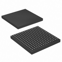
AT91CAP7E-NA-ZJ Atmel, AT91CAP7E-NA-ZJ Datasheet - Page 481

AT91CAP7E-NA-ZJ
Manufacturer Part Number
AT91CAP7E-NA-ZJ
Description
MCU CAP7 FPGA 225LFBGA
Manufacturer
Atmel
Series
CAP™r
Specifications of AT91CAP7E-NA-ZJ
Core Processor
ARM7
Core Size
16/32-Bit
Speed
80MHz
Connectivity
EBI/EMI, FPGA, IrDA, SPI, UART/USART, USB
Peripherals
DMA, POR, PWM, WDT
Number Of I /o
32
Program Memory Size
256KB (256K x 8)
Program Memory Type
ROM
Ram Size
160K x 8
Voltage - Supply (vcc/vdd)
1.08 V ~ 1.32 V
Data Converters
A/D 8x10b
Oscillator Type
Internal
Operating Temperature
-40°C ~ 85°C
Package / Case
225-LFBGA
Processor Series
AT91Mx
Core
ARM7TDMI
Data Bus Width
32 bit
3rd Party Development Tools
JTRACE-ARM-2M, MDK-ARM, RL-ARM, ULINK2
Lead Free Status / RoHS Status
Lead free / RoHS Compliant
Eeprom Size
-
Lead Free Status / Rohs Status
Details
Available stocks
Company
Part Number
Manufacturer
Quantity
Price
- Current page: 481 of 520
- Download datasheet (11Mb)
33. AT91CAP7E Electrical Characteristics
Note:
33.1
Table 33-1.
33.2
The following characteristics are applicable to the operating temperature range: T
ified and are certified for a junction temperature up to T
Table 33-2.
8549A–CAP–10/08
Operating Temperature (Industrial)-40⋅ C to +85⋅ C
Storage Temperature-60°C to +150°C
Voltage on Input Pins
with Respect to Ground-0.3V to +4.0V
Maximum Operating Voltage
(VDDCORE, VDDBU, VDDPLLB, VDDOSC, and
VDDOSC32)1.5V
Maximum Operating Voltage
(VDDIO, VDDPLLA, and AVDD)4.0V
Total DC Output Current on all I/O lines500 mA
Symbol
V
V
V
V
V
V
V
V
V
V
V
V
R
I
O
VDDCORE
VDDBU
VDDOSC
VDDOSC32
VDDPLLA
VDDPLLB
VDDIO
AVDD
IL
IH
OL
OH
PULLUP
This chapter contains preliminary values based on prototype silicon. These values are subject to change and will be recharac-
terized for the production silicon.
Absolute Maximum Ratings
DC Characteristics
Parameter
DC Supply Core
DC Supply Backup
DC Supply Oscillator
DC Supply 32kHz
Oscillator
DC Supply PLLA
DC Supply PLLB
DC Supply I/Os
DC Supply ADC
Input Low-level Voltage
Input High-level Voltage
Output Low-level Voltage
Output High-level Voltage
Pull-up Resistance
Output Current
Absolute Maximum Ratings*
DC Characteristics
Conditions
V
V
PA0-PA31
PA0-PA31
VDDIO
VDDIO
J
= 100°C.
*NOTICE:
Stresses beyond those listed under “Absolute Maximum
Ratings” may cause permanent damage to the device.
This is a stress rating only and functional operation of
the device at these or other conditions beyond those
indicated in the operational sections of this specification
is not implied. Exposure to absolute maximum rating
conditions for extended periods may affect device reli-
ability.
A
= -40°C to 85°C, unless otherwise spec-
V
VDDIO
1.08
1.08
1.08
1.08
1.08
Min
-0.3
3.0
3.0
3.0
40
2
-0.4
Typ
83
AT91CAP7E
V
VDDIO
Max
1.32
1.32
1.32
1.32
1.32
165
3.6
3.6
3.6
0.8
0.4
8
+0.3
kOhm
Units
mA
V
V
V
V
V
V
V
V
V
V
V
V
481
Related parts for AT91CAP7E-NA-ZJ
Image
Part Number
Description
Manufacturer
Datasheet
Request
R

Part Number:
Description:
Customizable Microcontroller
Manufacturer:
ATMEL Corporation
Datasheet:

Part Number:
Description:
DEV KIT FOR AVR/AVR32
Manufacturer:
Atmel
Datasheet:

Part Number:
Description:
INTERVAL AND WIPE/WASH WIPER CONTROL IC WITH DELAY
Manufacturer:
ATMEL Corporation
Datasheet:

Part Number:
Description:
Low-Voltage Voice-Switched IC for Hands-Free Operation
Manufacturer:
ATMEL Corporation
Datasheet:

Part Number:
Description:
MONOLITHIC INTEGRATED FEATUREPHONE CIRCUIT
Manufacturer:
ATMEL Corporation
Datasheet:

Part Number:
Description:
AM-FM Receiver IC U4255BM-M
Manufacturer:
ATMEL Corporation
Datasheet:

Part Number:
Description:
Monolithic Integrated Feature Phone Circuit
Manufacturer:
ATMEL Corporation
Datasheet:

Part Number:
Description:
Multistandard Video-IF and Quasi Parallel Sound Processing
Manufacturer:
ATMEL Corporation
Datasheet:

Part Number:
Description:
High-performance EE PLD
Manufacturer:
ATMEL Corporation
Datasheet:

Part Number:
Description:
8-bit Flash Microcontroller
Manufacturer:
ATMEL Corporation
Datasheet:

Part Number:
Description:
2-Wire Serial EEPROM
Manufacturer:
ATMEL Corporation
Datasheet:


