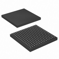
AT91CAP7E-NA-ZJ Atmel, AT91CAP7E-NA-ZJ Datasheet - Page 142

AT91CAP7E-NA-ZJ
Manufacturer Part Number
AT91CAP7E-NA-ZJ
Description
MCU CAP7 FPGA 225LFBGA
Manufacturer
Atmel
Series
CAP™r
Specifications of AT91CAP7E-NA-ZJ
Core Processor
ARM7
Core Size
16/32-Bit
Speed
80MHz
Connectivity
EBI/EMI, FPGA, IrDA, SPI, UART/USART, USB
Peripherals
DMA, POR, PWM, WDT
Number Of I /o
32
Program Memory Size
256KB (256K x 8)
Program Memory Type
ROM
Ram Size
160K x 8
Voltage - Supply (vcc/vdd)
1.08 V ~ 1.32 V
Data Converters
A/D 8x10b
Oscillator Type
Internal
Operating Temperature
-40°C ~ 85°C
Package / Case
225-LFBGA
Processor Series
AT91Mx
Core
ARM7TDMI
Data Bus Width
32 bit
3rd Party Development Tools
JTRACE-ARM-2M, MDK-ARM, RL-ARM, ULINK2
Lead Free Status / RoHS Status
Lead free / RoHS Compliant
Eeprom Size
-
Lead Free Status / Rohs Status
Details
Available stocks
Company
Part Number
Manufacturer
Quantity
Price
- Current page: 142 of 520
- Download datasheet (11Mb)
21.8.3
21.8.3.1
21.8.3.2
Figure 21-12. Write Cycle
142
AT91CAP7E
Write Waveforms
NWE Waveforms
NCS Waveforms
NBS0, NBS1,
NBS2, NBS3,
A0, A1
A [25:2]
MCK
NWE
NCS
The write protocol is similar to the read protocol. It is depicted in
starts with the address setting on the memory address bus.
The NWE signal is characterized by a setup timing, a pulse width and a hold timing.
The NWE waveforms apply to all byte-write lines in Byte Write access mode: NWR0 to NWR3.
The NCS signal waveforms in write operation are not the same that those applied in read opera-
tions, but are separately defined:
1. NWE_SETUP: the NWE setup time is defined as the setup of address and data before
2. NWE_PULSE: The NWE pulse length is the time between NWE falling edge and NWE
3. NWE_HOLD: The NWE hold time is defined as the hold time of address and data after
1. NCS_WR_SETUP: the NCS setup time is defined as the setup time of address before
2. NCS_WR_PULSE: the NCS pulse length is the time between NCS falling edge and
3. NCS_WR_HOLD: the NCS hold time is defined as the hold time of address after the
NCS_WR_SETUP
the NWE falling edge;
rising edge;
the NWE rising edge.
the NCS falling edge.
NCS rising edge;
NCS rising edge.
NWE_SETUP
NCS_WR_PULSE
NWE_CYCLE
NWE_PULSE
NWE_HOLD
NCS_WR_HOLD
Figure
21-12. The write cycle
8549A–CAP–10/08
Related parts for AT91CAP7E-NA-ZJ
Image
Part Number
Description
Manufacturer
Datasheet
Request
R

Part Number:
Description:
Customizable Microcontroller
Manufacturer:
ATMEL Corporation
Datasheet:

Part Number:
Description:
DEV KIT FOR AVR/AVR32
Manufacturer:
Atmel
Datasheet:

Part Number:
Description:
INTERVAL AND WIPE/WASH WIPER CONTROL IC WITH DELAY
Manufacturer:
ATMEL Corporation
Datasheet:

Part Number:
Description:
Low-Voltage Voice-Switched IC for Hands-Free Operation
Manufacturer:
ATMEL Corporation
Datasheet:

Part Number:
Description:
MONOLITHIC INTEGRATED FEATUREPHONE CIRCUIT
Manufacturer:
ATMEL Corporation
Datasheet:

Part Number:
Description:
AM-FM Receiver IC U4255BM-M
Manufacturer:
ATMEL Corporation
Datasheet:

Part Number:
Description:
Monolithic Integrated Feature Phone Circuit
Manufacturer:
ATMEL Corporation
Datasheet:

Part Number:
Description:
Multistandard Video-IF and Quasi Parallel Sound Processing
Manufacturer:
ATMEL Corporation
Datasheet:

Part Number:
Description:
High-performance EE PLD
Manufacturer:
ATMEL Corporation
Datasheet:

Part Number:
Description:
8-bit Flash Microcontroller
Manufacturer:
ATMEL Corporation
Datasheet:

Part Number:
Description:
2-Wire Serial EEPROM
Manufacturer:
ATMEL Corporation
Datasheet:


