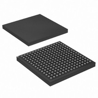
AT91CAP7E-NA-ZJ Atmel, AT91CAP7E-NA-ZJ Datasheet - Page 122

AT91CAP7E-NA-ZJ
Manufacturer Part Number
AT91CAP7E-NA-ZJ
Description
MCU CAP7 FPGA 225LFBGA
Manufacturer
Atmel
Series
CAP™r
Specifications of AT91CAP7E-NA-ZJ
Core Processor
ARM7
Core Size
16/32-Bit
Speed
80MHz
Connectivity
EBI/EMI, FPGA, IrDA, SPI, UART/USART, USB
Peripherals
DMA, POR, PWM, WDT
Number Of I /o
32
Program Memory Size
256KB (256K x 8)
Program Memory Type
ROM
Ram Size
160K x 8
Voltage - Supply (vcc/vdd)
1.08 V ~ 1.32 V
Data Converters
A/D 8x10b
Oscillator Type
Internal
Operating Temperature
-40°C ~ 85°C
Package / Case
225-LFBGA
Processor Series
AT91Mx
Core
ARM7TDMI
Data Bus Width
32 bit
3rd Party Development Tools
JTRACE-ARM-2M, MDK-ARM, RL-ARM, ULINK2
Lead Free Status / RoHS Status
Lead free / RoHS Compliant
Eeprom Size
-
Lead Free Status / Rohs Status
Details
Available stocks
Company
Part Number
Manufacturer
Quantity
Price
- Current page: 122 of 520
- Download datasheet (11Mb)
20.6
20.6.1
20.6.2
20.6.3
20.6.4
20.6.5
122
Functional Description
AT91CAP7E
Bus Multiplexing
Pull-up Control
Static Memory Controller
SDRAM Controller
CompactFlash Support
The EBI transfers data between the internal AHB Bus (handled by the Bus Matrix) and the exter-
nal memories or peripheral devices. It controls the waveforms and the parameters of the
external address, data and control busses and is composed of the following elements:
The EBI offers a complete set of control signals that share the 32-bit data lines, the address
lines of up to 26 bits and the control signals through a multiplex logic operating in function of the
memory area requests.
Multiplexing is specifically organized in order to guarantee the maintenance of the address and
output control lines at a stable state while no external access is being performed. Multiplexing is
also designed to respect the data float times defined in the Memory Controllers. Furthermore,
refresh cycles of the SDRAM are executed independently by the SDRAM Controller without
delaying the other external Memory Controller accesses.
The CSA register in the Bus Matrix User Interface permits enabling of on-chip pull-up resistors
on the data bus lines not multiplexed with the PIO Controller lines. The pull-up resistors are
enabled after reset. Setting the DBPUC bit disables the pull-up resistors on the D0 to D15 lines.
Enabling the pull-up resistor on the D16-D31 lines can be performed by programming the appro-
priate PIO controller.
For information on the Static Memory Controller, refer to the Static Memory Controller section.
For information on the SDRAM Controller, refer to the SDRAM section.
The External Bus Interface integrates circuitry that interfaces to CompactFlash devices.
The CompactFlash logic is driven by the Static Memory Controller (SMC) on the NCS4 and/or
NCS5 address space. Programming the CS4A and/or CS5A bit of the CSA Register to the
appropriate value enables this logic. For details on this register, refer to the Bus Matrix User
Interface section. Access to an external CompactFlash device is then made by accessing the
address space reserved to NCS4 and/or NCS5 (i.e., between 0x5000 0000 and 0x5FFF FFFF
for NCS4 and between 0x6000 0000 and 0x6FFF FFFF for NCS5).
All CompactFlash modes (Attribute Memory, Common Memory, I/O and True IDE) are sup-
ported but the signals _IOIS16 (I/O and True IDE modes) and _ATA SEL (True IDE mode) are
not handled.
• Static Memory Controller (SMC)
• SDRAM Controller (SDRAMC)
• A chip select assignment feature that assigns an AHB address space to the external devices
• A multiplex controller circuit that shares the pins between the different Memory Controllers
• Programmable CompactFlash support logic
• Programmable NAND Flash support logic
8549A–CAP–10/08
Related parts for AT91CAP7E-NA-ZJ
Image
Part Number
Description
Manufacturer
Datasheet
Request
R

Part Number:
Description:
Customizable Microcontroller
Manufacturer:
ATMEL Corporation
Datasheet:

Part Number:
Description:
DEV KIT FOR AVR/AVR32
Manufacturer:
Atmel
Datasheet:

Part Number:
Description:
INTERVAL AND WIPE/WASH WIPER CONTROL IC WITH DELAY
Manufacturer:
ATMEL Corporation
Datasheet:

Part Number:
Description:
Low-Voltage Voice-Switched IC for Hands-Free Operation
Manufacturer:
ATMEL Corporation
Datasheet:

Part Number:
Description:
MONOLITHIC INTEGRATED FEATUREPHONE CIRCUIT
Manufacturer:
ATMEL Corporation
Datasheet:

Part Number:
Description:
AM-FM Receiver IC U4255BM-M
Manufacturer:
ATMEL Corporation
Datasheet:

Part Number:
Description:
Monolithic Integrated Feature Phone Circuit
Manufacturer:
ATMEL Corporation
Datasheet:

Part Number:
Description:
Multistandard Video-IF and Quasi Parallel Sound Processing
Manufacturer:
ATMEL Corporation
Datasheet:

Part Number:
Description:
High-performance EE PLD
Manufacturer:
ATMEL Corporation
Datasheet:

Part Number:
Description:
8-bit Flash Microcontroller
Manufacturer:
ATMEL Corporation
Datasheet:

Part Number:
Description:
2-Wire Serial EEPROM
Manufacturer:
ATMEL Corporation
Datasheet:


