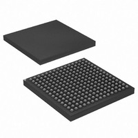
AT91CAP7E-NA-ZJ Atmel, AT91CAP7E-NA-ZJ Datasheet - Page 18

AT91CAP7E-NA-ZJ
Manufacturer Part Number
AT91CAP7E-NA-ZJ
Description
MCU CAP7 FPGA 225LFBGA
Manufacturer
Atmel
Series
CAP™r
Specifications of AT91CAP7E-NA-ZJ
Core Processor
ARM7
Core Size
16/32-Bit
Speed
80MHz
Connectivity
EBI/EMI, FPGA, IrDA, SPI, UART/USART, USB
Peripherals
DMA, POR, PWM, WDT
Number Of I /o
32
Program Memory Size
256KB (256K x 8)
Program Memory Type
ROM
Ram Size
160K x 8
Voltage - Supply (vcc/vdd)
1.08 V ~ 1.32 V
Data Converters
A/D 8x10b
Oscillator Type
Internal
Operating Temperature
-40°C ~ 85°C
Package / Case
225-LFBGA
Processor Series
AT91Mx
Core
ARM7TDMI
Data Bus Width
32 bit
3rd Party Development Tools
JTRACE-ARM-2M, MDK-ARM, RL-ARM, ULINK2
Lead Free Status / RoHS Status
Lead free / RoHS Compliant
Eeprom Size
-
Lead Free Status / Rohs Status
Details
Available stocks
Company
Part Number
Manufacturer
Quantity
Price
- Current page: 18 of 520
- Download datasheet (11Mb)
8. Memories
8.1
8.2
Figure 8-1.
18
Embedded Memories
Memory Mapping
AT91CAP7E
AT91CAP7E Product Memory Mapping
8 x 256M Bytes
2,048M bytes
6 x 256M Bytes
A first level of address decoding is performed by the Bus Matrix, i.e., the implementation of the
Advanced High performance Bus (AHB) for its Master and Slave interfaces with additional
features.
Decoding breaks up the 4G bytes of address space into 16 banks of 256M bytes. The banks 1 to
9 are directed to the EBI that associates these banks to the external chip selects NCS0 to
NCS7. The bank 0 is reserved for the addressing of the internal memories, and a second level of
decoding provides 1M byte of internal memory area. The bank 15 is reserved for the peripherals
and provides access to the Advanced Peripheral Bus (APB).
Other areas are unused and performing an access within them provides an abort to the master
requesting such an access.
Each Master has its own bus and its own decoder, thus allowing a different memory mapping
per Master. However, in order to simplify the mappings, all the masters have a similar address
decoding.
Regarding Master 0 (ARM7TDMI), two different Slaves are assigned to the memory space
decoded at address 0x0: one for internal boot and one for external boot.
256M Bytes
1,536M Bytes
256M Bytes
• 256 Kbyte Fast ROM
• 96 Kbyte Fast SRAM
• 64 Kbyte Fast SRAM
– Single Cycle Access at full matrix speed
– Single Cycle Access at full matrix speed
– Single Cycle Access at full matrix speed
0x0000 0000
0x1000 0000
0x9000 0000
0xF000 0000
0xEFFF FFFF
0xFFFF FFFF
0x0FFF FFFF
0x8FFF FFFF
External Bus Interface
Internal Peripherals
Internal Memories
Chip Select 0 to 7
Undefined
(Abort)
8549A–CAP–10/08
Related parts for AT91CAP7E-NA-ZJ
Image
Part Number
Description
Manufacturer
Datasheet
Request
R

Part Number:
Description:
Customizable Microcontroller
Manufacturer:
ATMEL Corporation
Datasheet:

Part Number:
Description:
DEV KIT FOR AVR/AVR32
Manufacturer:
Atmel
Datasheet:

Part Number:
Description:
INTERVAL AND WIPE/WASH WIPER CONTROL IC WITH DELAY
Manufacturer:
ATMEL Corporation
Datasheet:

Part Number:
Description:
Low-Voltage Voice-Switched IC for Hands-Free Operation
Manufacturer:
ATMEL Corporation
Datasheet:

Part Number:
Description:
MONOLITHIC INTEGRATED FEATUREPHONE CIRCUIT
Manufacturer:
ATMEL Corporation
Datasheet:

Part Number:
Description:
AM-FM Receiver IC U4255BM-M
Manufacturer:
ATMEL Corporation
Datasheet:

Part Number:
Description:
Monolithic Integrated Feature Phone Circuit
Manufacturer:
ATMEL Corporation
Datasheet:

Part Number:
Description:
Multistandard Video-IF and Quasi Parallel Sound Processing
Manufacturer:
ATMEL Corporation
Datasheet:

Part Number:
Description:
High-performance EE PLD
Manufacturer:
ATMEL Corporation
Datasheet:

Part Number:
Description:
8-bit Flash Microcontroller
Manufacturer:
ATMEL Corporation
Datasheet:

Part Number:
Description:
2-Wire Serial EEPROM
Manufacturer:
ATMEL Corporation
Datasheet:


