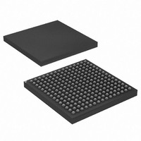
AT91CAP7E-NA-ZJ Atmel, AT91CAP7E-NA-ZJ Datasheet - Page 41

AT91CAP7E-NA-ZJ
Manufacturer Part Number
AT91CAP7E-NA-ZJ
Description
MCU CAP7 FPGA 225LFBGA
Manufacturer
Atmel
Series
CAP™r
Specifications of AT91CAP7E-NA-ZJ
Core Processor
ARM7
Core Size
16/32-Bit
Speed
80MHz
Connectivity
EBI/EMI, FPGA, IrDA, SPI, UART/USART, USB
Peripherals
DMA, POR, PWM, WDT
Number Of I /o
32
Program Memory Size
256KB (256K x 8)
Program Memory Type
ROM
Ram Size
160K x 8
Voltage - Supply (vcc/vdd)
1.08 V ~ 1.32 V
Data Converters
A/D 8x10b
Oscillator Type
Internal
Operating Temperature
-40°C ~ 85°C
Package / Case
225-LFBGA
Processor Series
AT91Mx
Core
ARM7TDMI
Data Bus Width
32 bit
3rd Party Development Tools
JTRACE-ARM-2M, MDK-ARM, RL-ARM, ULINK2
Lead Free Status / RoHS Status
Lead free / RoHS Compliant
Eeprom Size
-
Lead Free Status / Rohs Status
Details
Available stocks
Company
Part Number
Manufacturer
Quantity
Price
- Current page: 41 of 520
- Download datasheet (11Mb)
11. FPGA Interface (FPIF)
11.1
11.2
8549A–CAP–10/08
Description
System Requirements and Integration
The FPGA Interface (FPIF) module provides a means to connect an external FPGA directly to
the AT91CAP7E internal AHB Bus. This interface is implemented in the metal-programmable
logic block (MP Block) that is provided as part of the AT91CAP7S customizable microcontroller
platform. Therefore the interface is constrained to access the AHB Bus through the Masters and
Slaves already pre-defined for the MP block.
The FPGA interface is implemented using several serializers that encode/decode all the traffic
between the CAP7E and the FPGA. In order to have proper communication and synchronization
between both devices, the following requirements must be met:
ATMEL provides some examples of how to integrate logic in the FPGA using the CAP7E FPGA
interface.
•
•
•
•
•
•
•
•
•
1. The FPGA being connected to CAP7E must be capable of handling skew clock balancing
2. The FPGA must provide the configuration modes and a reset to the CAP7E.
3. The FPGA must provide the serial communication clock to CAP7E.
4. The frequency for the serializer clock can be as fast as 100Mhz for the commercial tem-
5. The ratio between the internal CAP7E AHB Master Clock (MCK) and the FPGA Interface
6. All the logic added to the FPGA must utilize the Atmel-provided encoding/decoding logic
7. A template is provided to instantiate the AHB Masters and Slaves with the FPGA inter-
The FPGA interface uses 82 of the metal-programmable I/O pads (MPIO’s) provided on
the CAP7 platform, and it provides FPGA access to the following MP block features:
2 AHB Masters
4 AHB Slaves
1 AHB Slave to remap the ROM using an external ZBT RAM through the FPGA (For
CAP7 Emulation purposes). Programmable ROM remap feature at startup.
14 APB’s slaves
2 DMA full duplex channels
Up to 13 priority encoded IRQ’s
2 unencoded IRQ’s for DMA transfers
32 bits PIO (Shared I/O)
and latency cancellation. For example in a Xilinx FPGA, the use of DCM’s is mandatory.
perature/voltage/process range.
Serial Clock (FPIF_SCLK) should be approximately 0.8 or lower (MCK / FPIF_SCLK).
to ensure proper communication with CAP7E. Currently only Altera and Xilinx FPGA’s
are supported, but other FPGA’s may be supported in the future.
face.
Figure 11-1
shows a system diagram of the CAP7E and an FPGA.
AT91CAP7E
41
Related parts for AT91CAP7E-NA-ZJ
Image
Part Number
Description
Manufacturer
Datasheet
Request
R

Part Number:
Description:
Customizable Microcontroller
Manufacturer:
ATMEL Corporation
Datasheet:

Part Number:
Description:
DEV KIT FOR AVR/AVR32
Manufacturer:
Atmel
Datasheet:

Part Number:
Description:
INTERVAL AND WIPE/WASH WIPER CONTROL IC WITH DELAY
Manufacturer:
ATMEL Corporation
Datasheet:

Part Number:
Description:
Low-Voltage Voice-Switched IC for Hands-Free Operation
Manufacturer:
ATMEL Corporation
Datasheet:

Part Number:
Description:
MONOLITHIC INTEGRATED FEATUREPHONE CIRCUIT
Manufacturer:
ATMEL Corporation
Datasheet:

Part Number:
Description:
AM-FM Receiver IC U4255BM-M
Manufacturer:
ATMEL Corporation
Datasheet:

Part Number:
Description:
Monolithic Integrated Feature Phone Circuit
Manufacturer:
ATMEL Corporation
Datasheet:

Part Number:
Description:
Multistandard Video-IF and Quasi Parallel Sound Processing
Manufacturer:
ATMEL Corporation
Datasheet:

Part Number:
Description:
High-performance EE PLD
Manufacturer:
ATMEL Corporation
Datasheet:

Part Number:
Description:
8-bit Flash Microcontroller
Manufacturer:
ATMEL Corporation
Datasheet:

Part Number:
Description:
2-Wire Serial EEPROM
Manufacturer:
ATMEL Corporation
Datasheet:


