DF2214BQ16V Renesas Electronics America, DF2214BQ16V Datasheet - Page 703
DF2214BQ16V
Manufacturer Part Number
DF2214BQ16V
Description
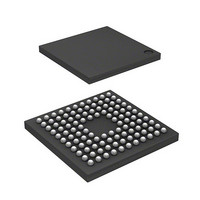
IC H8S/2214 MCU FLASH 112-TFBGA
Manufacturer
Renesas Electronics America
Series
H8® H8S/2200r
Datasheets
1.HS2214ECB62H.pdf
(938 pages)
2.HEWH8E10A.pdf
(19 pages)
3.D12312SVTE25V.pdf
(341 pages)
Specifications of DF2214BQ16V
Core Processor
H8S/2000
Core Size
16-Bit
Speed
16MHz
Connectivity
SCI
Peripherals
DMA, POR, PWM, WDT
Number Of I /o
72
Program Memory Size
128KB (128K x 8)
Program Memory Type
FLASH
Ram Size
12K x 8
Voltage - Supply (vcc/vdd)
2.7 V ~ 3.6 V
Data Converters
D/A 1x8b
Oscillator Type
Internal
Operating Temperature
-20°C ~ 75°C
Package / Case
112-TFBGA
For Use With
HS0005KCU11H - EMULATOR E10A-USB H8S(X),SH2(A)3DK2218 - DEV EVAL KIT H8S/2218
Lead Free Status / RoHS Status
Lead free / RoHS Compliant
Eeprom Size
-
Available stocks
Company
Part Number
Manufacturer
Quantity
Price
Company:

Part Number:
DF2214BQ16V
Manufacturer:
Renesas Electronics America
Quantity:
10 000


Notes: 1. If the D/A converter is not used, do not leave the AV
Table 18.5 Permissible Output Currents
Conditions: V
Item
Permissible output
high current (total)
Note: * To protect chip reliability, do not exceed the output current values in table 18.5.
Permissible output
low current (per pin)
Permissible output
low current (total)
Permissible output
high current (per pin)
2. Current dissipation values are for V
3. The values are for V
4. I
voltage between 2.0 V and 3.6 V to the AV
instance. Set V
output pins unloaded and the on-chip pull-up resistors in the off state.
I
I
CC
CC
CC
T
T
depends on V
(max.) = 1.0 (mA) + 0.61 (mA/(MHz × V)) × V
(max.) = 1.0 (mA) + 0.44 (mA/(MHz × V)) × V
a
a
CC
= –20°C to +75°C (regular specifications),
= –40°C to +85°C (wide-range specifications) *
= 2.7 V to 3.6 V, AV
Total of all
output pins
All output
pins
Total of all
output pins
All output
pins
ref
CC
= AV
and f as follows:
RAM
CC
≤ V
.
V
V
V
V
CC
CC
CC
CC
CC
CC
= 2.7 to 3.6 V
= 2.7 to 3.6 V
= 2.7 to 3.6 V
= 2.7 to 3.6 V
< 2.7 V, V
= 2.7 V to 3.6 V, V
IH
(min.) = V
IH
(min.) = V
CC
and V
Symbol Min.
∑ –I
I
∑ I
–I
Rev.4.00 Sep. 18, 2008 Page 641 of 872
OL
CC
OH
CC
CC
OL
– 0.3 V, V
OH
ref
× f (normal operation)
× f (sleep mode)
Section 18 Electrical Characteristics
ref
CC
= AV
CC
pins by connecting them to V
× 0.9, and V
, V
—
—
—
—
ref
CC
, and AV
, V
IL
(max.) = 0.3 V with all
SS
Typ.
—
—
—
—
= AV
IL
SS
(max.) = 0.3 V.
pins open. Apply a
REJ09B0189-0400
SS
= 0 V,
Max.
30
1.0
60
1.0
Unit
mA
mA
mA
mA
CC
, for
Related parts for DF2214BQ16V
Image
Part Number
Description
Manufacturer
Datasheet
Request
R

Part Number:
Description:
CONN SOCKET 2POS 7.92MM WHITE
Manufacturer:
Hirose Electric Co Ltd
Datasheet:

Part Number:
Description:
CONN SOCKET 4POS 7.92MM WHITE
Manufacturer:
Hirose Electric Co Ltd
Datasheet:

Part Number:
Description:
CONN SOCKET 5POS 7.92MM WHITE
Manufacturer:
Hirose Electric Co Ltd
Datasheet:

Part Number:
Description:
CONN SOCKET 3POS 7.92MM WHITE
Manufacturer:
Hirose Electric Co Ltd
Datasheet:
Part Number:
Description:
CONN SOCKET 5POS 7.92MM WHITE
Manufacturer:
Hirose Electric Co Ltd
Datasheet:

Part Number:
Description:
CONN SOCKET 2POS 7.92MM WHITE
Manufacturer:
Hirose Electric Co Ltd
Datasheet:
Part Number:
Description:
CONN SOCKET 3POS 7.92MM WHITE
Manufacturer:
Hirose Electric Co Ltd
Datasheet:
Part Number:
Description:
CONN SOCKET 4POS 7.92MM WHITE
Manufacturer:
Hirose Electric Co Ltd
Datasheet:

Part Number:
Description:
CONN HEADER 2POS 7.92MM R/A TIN
Manufacturer:
Hirose Electric Co Ltd
Datasheet:

Part Number:
Description:
CONN HEADER 4POS 7.92MM R/A TIN
Manufacturer:
Hirose Electric Co Ltd
Datasheet:

Part Number:
Description:
KIT STARTER FOR M16C/29
Manufacturer:
Renesas Electronics America
Datasheet:

Part Number:
Description:
KIT STARTER FOR R8C/2D
Manufacturer:
Renesas Electronics America
Datasheet:

Part Number:
Description:
R0K33062P STARTER KIT
Manufacturer:
Renesas Electronics America
Datasheet:

Part Number:
Description:
KIT STARTER FOR R8C/23 E8A
Manufacturer:
Renesas Electronics America
Datasheet:

Part Number:
Description:
KIT STARTER FOR R8C/25
Manufacturer:
Renesas Electronics America
Datasheet: