DF2214BQ16V Renesas Electronics America, DF2214BQ16V Datasheet - Page 44
DF2214BQ16V
Manufacturer Part Number
DF2214BQ16V
Description
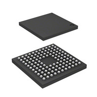
IC H8S/2214 MCU FLASH 112-TFBGA
Manufacturer
Renesas Electronics America
Series
H8® H8S/2200r
Datasheets
1.HS2214ECB62H.pdf
(938 pages)
2.HEWH8E10A.pdf
(19 pages)
3.D12312SVTE25V.pdf
(341 pages)
Specifications of DF2214BQ16V
Core Processor
H8S/2000
Core Size
16-Bit
Speed
16MHz
Connectivity
SCI
Peripherals
DMA, POR, PWM, WDT
Number Of I /o
72
Program Memory Size
128KB (128K x 8)
Program Memory Type
FLASH
Ram Size
12K x 8
Voltage - Supply (vcc/vdd)
2.7 V ~ 3.6 V
Data Converters
D/A 1x8b
Oscillator Type
Internal
Operating Temperature
-20°C ~ 75°C
Package / Case
112-TFBGA
For Use With
HS0005KCU11H - EMULATOR E10A-USB H8S(X),SH2(A)3DK2218 - DEV EVAL KIT H8S/2218
Lead Free Status / RoHS Status
Lead free / RoHS Compliant
Eeprom Size
-
Available stocks
Company
Part Number
Manufacturer
Quantity
Price
Company:

Part Number:
DF2214BQ16V
Manufacturer:
Renesas Electronics America
Quantity:
10 000


15.14 Flash Memory and Power-Down States............................................................................. 597
15.15 Flash Memory Programming and Erasing Precautions...................................................... 598
15.16 Note on Switching from F-ZTAT Version to Masked ROM Version ............................... 604
Section 16 Clock Pulse Generator .....................................................................605
16.1 Overview............................................................................................................................ 605
16.2 Register Descriptions ......................................................................................................... 606
16.3 System Clock Oscillator..................................................................................................... 609
16.4 Duty Adjustment Circuit.................................................................................................... 615
16.5 Medium-Speed Clock Divider ........................................................................................... 615
16.6 Bus Master Clock Selection Circuit................................................................................... 615
16.7 Note on Crystal Resonator ................................................................................................. 615
Section 17 Power-Down Modes ........................................................................617
17.1 Overview............................................................................................................................ 617
17.2 Register Descriptions ......................................................................................................... 620
17.3 Medium-Speed Mode......................................................................................................... 624
17.4 Sleep Mode ........................................................................................................................ 625
17.5 Module Stop Mode ............................................................................................................ 626
Rev.4.00 Sep. 18, 2008 Page xlii of lx
REJ09B0189-0400
15.13.1 Socket Adapter Pin Correspondence Diagram...................................................... 583
15.13.2 Programmer Mode Operation ............................................................................... 585
15.13.3 Memory Read Mode ............................................................................................. 586
15.13.4 Auto-Program Mode ............................................................................................. 590
15.13.5 Auto-Erase Mode.................................................................................................. 592
15.13.6 Status Read Mode ................................................................................................. 594
15.13.7 Status Polling ........................................................................................................ 595
15.13.8 Programmer Mode Transition Time ..................................................................... 596
15.13.9 Notes on Memory Programming........................................................................... 597
15.14.1 Note on Power-Down States ................................................................................. 598
16.1.1 Block Diagram...................................................................................................... 605
16.1.2 Register Configuration.......................................................................................... 606
16.2.1 System Clock Control Register (SCKCR) ............................................................ 606
16.2.2 Low-Power Control Register (LPWRCR) ............................................................ 607
16.3.1 Connecting a Crystal Resonator............................................................................ 609
16.3.2 External Clock Input............................................................................................. 611
17.1.1 Register Configuration.......................................................................................... 620
17.2.1 Standby Control Register (SBYCR) ..................................................................... 620
17.2.2 System Clock Control Register (SCKCR) ............................................................ 622
17.2.3 Module Stop Control Register (MSTPCR) ........................................................... 623
17.4.1 Sleep Mode ........................................................................................................... 625
17.4.2 Clearing Sleep Mode............................................................................................. 625
Related parts for DF2214BQ16V
Image
Part Number
Description
Manufacturer
Datasheet
Request
R

Part Number:
Description:
CONN SOCKET 2POS 7.92MM WHITE
Manufacturer:
Hirose Electric Co Ltd
Datasheet:

Part Number:
Description:
CONN SOCKET 4POS 7.92MM WHITE
Manufacturer:
Hirose Electric Co Ltd
Datasheet:

Part Number:
Description:
CONN SOCKET 5POS 7.92MM WHITE
Manufacturer:
Hirose Electric Co Ltd
Datasheet:

Part Number:
Description:
CONN SOCKET 3POS 7.92MM WHITE
Manufacturer:
Hirose Electric Co Ltd
Datasheet:
Part Number:
Description:
CONN SOCKET 5POS 7.92MM WHITE
Manufacturer:
Hirose Electric Co Ltd
Datasheet:

Part Number:
Description:
CONN SOCKET 2POS 7.92MM WHITE
Manufacturer:
Hirose Electric Co Ltd
Datasheet:
Part Number:
Description:
CONN SOCKET 3POS 7.92MM WHITE
Manufacturer:
Hirose Electric Co Ltd
Datasheet:
Part Number:
Description:
CONN SOCKET 4POS 7.92MM WHITE
Manufacturer:
Hirose Electric Co Ltd
Datasheet:

Part Number:
Description:
CONN HEADER 2POS 7.92MM R/A TIN
Manufacturer:
Hirose Electric Co Ltd
Datasheet:

Part Number:
Description:
CONN HEADER 4POS 7.92MM R/A TIN
Manufacturer:
Hirose Electric Co Ltd
Datasheet:

Part Number:
Description:
KIT STARTER FOR M16C/29
Manufacturer:
Renesas Electronics America
Datasheet:

Part Number:
Description:
KIT STARTER FOR R8C/2D
Manufacturer:
Renesas Electronics America
Datasheet:

Part Number:
Description:
R0K33062P STARTER KIT
Manufacturer:
Renesas Electronics America
Datasheet:

Part Number:
Description:
KIT STARTER FOR R8C/23 E8A
Manufacturer:
Renesas Electronics America
Datasheet:

Part Number:
Description:
KIT STARTER FOR R8C/25
Manufacturer:
Renesas Electronics America
Datasheet: