DF2214BQ16V Renesas Electronics America, DF2214BQ16V Datasheet - Page 18
DF2214BQ16V
Manufacturer Part Number
DF2214BQ16V
Description
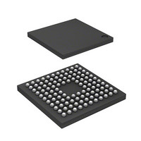
IC H8S/2214 MCU FLASH 112-TFBGA
Manufacturer
Renesas Electronics America
Series
H8® H8S/2200r
Datasheets
1.HS2214ECB62H.pdf
(938 pages)
2.HEWH8E10A.pdf
(19 pages)
3.D12312SVTE25V.pdf
(341 pages)
Specifications of DF2214BQ16V
Core Processor
H8S/2000
Core Size
16-Bit
Speed
16MHz
Connectivity
SCI
Peripherals
DMA, POR, PWM, WDT
Number Of I /o
72
Program Memory Size
128KB (128K x 8)
Program Memory Type
FLASH
Ram Size
12K x 8
Voltage - Supply (vcc/vdd)
2.7 V ~ 3.6 V
Data Converters
D/A 1x8b
Oscillator Type
Internal
Operating Temperature
-20°C ~ 75°C
Package / Case
112-TFBGA
For Use With
HS0005KCU11H - EMULATOR E10A-USB H8S(X),SH2(A)3DK2218 - DEV EVAL KIT H8S/2218
Lead Free Status / RoHS Status
Lead free / RoHS Compliant
Eeprom Size
-
Available stocks
Company
Part Number
Manufacturer
Quantity
Price
Company:

Part Number:
DF2214BQ16V
Manufacturer:
Renesas Electronics America
Quantity:
10 000


Item
12.2.7 Serial
Status Register
(SSR)
Bit 2—Transmit End
(TEND)
12.3.2 Operation in
Asynchronous Mode
Figure 12.7
Sample SCI
Initialization
Flowchart
Rev.4.00 Sep. 18, 2008 Page xvi of lx
REJ09B0189-0400
Page
470
493
Revisions (See Manual for Details)
Note added
Bit 2
TEND
0
Note: * This bit is cleared by DTC when DISEL = 0 and
Note added
Set CKE1 and CKE0 bits in SCR
SCR to 1, and set RIE, TIE, TEIE,
Clear TE and RE bits in SCR to 0
Set data transfer format in
Set TE and RE* bits in
<Transfer completion>
1-bit interval elapsed?
SMR and SCMR
Start initialization
Set value in BRR
Description
[Clearing conditions]
•
•
(TE, RE bits 0)
and MPIE bits
furthermore the transfer counter is not 0.
When 0 is written to TDRE after reading TDRE = 1
When the DMAC or DTC* is activated by a TXI interrupt and writes data to TDR
Yes
Wait
No
[1]
[2]
[3]
[4]
[1] Set the clock selection in SCR.
[2] Set the data transfer format in SMR
[3] Write a value corresponding to the
[4] Wait at least one bit interval, then
Note: * The RE bit must be set when
Be sure to clear bits RIE, TIE,
TEIE, and MPIE, and bits TE and
RE, to 0.
When the clock is selected in
asynchronous mode, it is output
immediately after SCR settings are
made.
and SCMR.
bit rate to BRR. Not necessary if an
external clock is used.
set the TE bit or RE bit in SCR to 1.
Also set the RIE, TIE, TEIE, and
MPIE bits.
Setting the TE and RE bits enables
the TxD and RxD pins to be used.
the RxD pin is in the 1 state. If
the RE bit is set t 1 with the
RxD pin in the 0 state, this
event may be mistakenly
recognized as a start bit.
Related parts for DF2214BQ16V
Image
Part Number
Description
Manufacturer
Datasheet
Request
R

Part Number:
Description:
CONN SOCKET 2POS 7.92MM WHITE
Manufacturer:
Hirose Electric Co Ltd
Datasheet:

Part Number:
Description:
CONN SOCKET 4POS 7.92MM WHITE
Manufacturer:
Hirose Electric Co Ltd
Datasheet:

Part Number:
Description:
CONN SOCKET 5POS 7.92MM WHITE
Manufacturer:
Hirose Electric Co Ltd
Datasheet:

Part Number:
Description:
CONN SOCKET 3POS 7.92MM WHITE
Manufacturer:
Hirose Electric Co Ltd
Datasheet:
Part Number:
Description:
CONN SOCKET 5POS 7.92MM WHITE
Manufacturer:
Hirose Electric Co Ltd
Datasheet:

Part Number:
Description:
CONN SOCKET 2POS 7.92MM WHITE
Manufacturer:
Hirose Electric Co Ltd
Datasheet:
Part Number:
Description:
CONN SOCKET 3POS 7.92MM WHITE
Manufacturer:
Hirose Electric Co Ltd
Datasheet:
Part Number:
Description:
CONN SOCKET 4POS 7.92MM WHITE
Manufacturer:
Hirose Electric Co Ltd
Datasheet:

Part Number:
Description:
CONN HEADER 2POS 7.92MM R/A TIN
Manufacturer:
Hirose Electric Co Ltd
Datasheet:

Part Number:
Description:
CONN HEADER 4POS 7.92MM R/A TIN
Manufacturer:
Hirose Electric Co Ltd
Datasheet:

Part Number:
Description:
KIT STARTER FOR M16C/29
Manufacturer:
Renesas Electronics America
Datasheet:

Part Number:
Description:
KIT STARTER FOR R8C/2D
Manufacturer:
Renesas Electronics America
Datasheet:

Part Number:
Description:
R0K33062P STARTER KIT
Manufacturer:
Renesas Electronics America
Datasheet:

Part Number:
Description:
KIT STARTER FOR R8C/23 E8A
Manufacturer:
Renesas Electronics America
Datasheet:

Part Number:
Description:
KIT STARTER FOR R8C/25
Manufacturer:
Renesas Electronics America
Datasheet: