DF2214BQ16V Renesas Electronics America, DF2214BQ16V Datasheet - Page 49
DF2214BQ16V
Manufacturer Part Number
DF2214BQ16V
Description
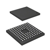
IC H8S/2214 MCU FLASH 112-TFBGA
Manufacturer
Renesas Electronics America
Series
H8® H8S/2200r
Datasheets
1.HS2214ECB62H.pdf
(938 pages)
2.HEWH8E10A.pdf
(19 pages)
3.D12312SVTE25V.pdf
(341 pages)
Specifications of DF2214BQ16V
Core Processor
H8S/2000
Core Size
16-Bit
Speed
16MHz
Connectivity
SCI
Peripherals
DMA, POR, PWM, WDT
Number Of I /o
72
Program Memory Size
128KB (128K x 8)
Program Memory Type
FLASH
Ram Size
12K x 8
Voltage - Supply (vcc/vdd)
2.7 V ~ 3.6 V
Data Converters
D/A 1x8b
Oscillator Type
Internal
Operating Temperature
-20°C ~ 75°C
Package / Case
112-TFBGA
For Use With
HS0005KCU11H - EMULATOR E10A-USB H8S(X),SH2(A)3DK2218 - DEV EVAL KIT H8S/2218
Lead Free Status / RoHS Status
Lead free / RoHS Compliant
Eeprom Size
-
Available stocks
Company
Part Number
Manufacturer
Quantity
Price
Company:

Part Number:
DF2214BQ16V
Manufacturer:
Renesas Electronics America
Quantity:
10 000


Figure 6.23 On-Chip ROM Valid Extended Mode (Mode 6) Address Map............................... 172
Section 7 DMA Controller
Figure 7.1
Figure 7.2
Figure 7.3
Figure 7.4
Figure 7.5
Figure 7.6
Figure 7.7
Figure 7.8
Figure 7.9
Figure 7.10 Example of Normal Mode Setting Procedure.......................................................... 223
Figure 7.11 Operation in Block Transfer Mode (BLKDIR = 0) ................................................. 225
Figure 7.12 Operation in Block Transfer Mode (BLKDIR = 1) ................................................. 226
Figure 7.13 Operation Flow in Block Transfer Mode ................................................................ 228
Figure 7.14 Example of Block Transfer Mode Setting Procedure.............................................. 229
Figure 7.15 Example of DMA Transfer Bus Timing.................................................................. 232
Figure 7.16 Example of Short Address Mode Transfer .............................................................. 233
Figure 7.17 Example of Full Address Mode (Cycle Steal) Transfer .......................................... 234
Figure 7.18 Example of Full Address Mode (Burst Mode) Transfer.......................................... 235
Figure 7.19 Example of Full Address Mode (Block Transfer Mode) Transfer .......................... 236
Figure 7.20 Example of DREQ Pin Falling Edge Activated Normal Mode Transfer................. 237
Figure 7.21 Example of DREQ Pin Falling Edge Activated Block Transfer Mode Transfer..... 238
Figure 7.22 Example of DREQ Level Activated Normal Mode Transfer .................................. 239
Figure 7.23 Example of DREQ Level Activated Block Transfer Mode Transfer ...................... 240
Figure 7.24 Example of Multi-Channel Transfer ....................................................................... 241
Figure 7.25 Example of Procedure for Continuing Transfer on Channel Interrupted
Figure 7.26 Example of Procedure for Forcibly Terminating DMAC Operation....................... 244
Figure 7.27 Example of Procedure for Clearing Full Address Mode ......................................... 245
Figure 7.28 Block Diagram of Transfer End/Transfer Break Interrupt ...................................... 246
Figure 7.29 DMAC Register Update Timing ............................................................................. 247
Figure 7.30 Contention between DMAC Register Update and CPU Read................................. 248
Section 8 Data Transfer Controller (DTC)
Figure 8.1
Figure 8.2
Figure 8.3
Figure 8.4
Figure 8.5
Correspondence between DTC Vector Address and Register Information ............. 268
Block Diagram of DMAC ....................................................................................... 174
Areas for Register Re-Setting by DTC (Example: Channel 0A)............................. 204
Operation in Sequential Mode................................................................................. 212
Example of Sequential Mode Setting Procedure ..................................................... 213
Operation in Idle Mode ........................................................................................... 215
Example of Idle Mode Setting Procedure................................................................ 216
Operation in Repeat mode....................................................................................... 219
Example of Repeat Mode Setting Procedure........................................................... 220
Operation in Normal Mode ..................................................................................... 222
by NMI Interrupt ..................................................................................................... 243
Block Diagram of DTC ........................................................................................... 252
Flowchart of DTC Operation................................................................................... 262
Block Diagram of DTC Activation Source Control ................................................ 265
Location of Register Information in Address Space................................................ 268
Rev.4.00 Sep. 18, 2008 Page xlvii of lx
REJ09B0189-0400
Related parts for DF2214BQ16V
Image
Part Number
Description
Manufacturer
Datasheet
Request
R

Part Number:
Description:
CONN SOCKET 2POS 7.92MM WHITE
Manufacturer:
Hirose Electric Co Ltd
Datasheet:

Part Number:
Description:
CONN SOCKET 4POS 7.92MM WHITE
Manufacturer:
Hirose Electric Co Ltd
Datasheet:

Part Number:
Description:
CONN SOCKET 5POS 7.92MM WHITE
Manufacturer:
Hirose Electric Co Ltd
Datasheet:

Part Number:
Description:
CONN SOCKET 3POS 7.92MM WHITE
Manufacturer:
Hirose Electric Co Ltd
Datasheet:
Part Number:
Description:
CONN SOCKET 5POS 7.92MM WHITE
Manufacturer:
Hirose Electric Co Ltd
Datasheet:

Part Number:
Description:
CONN SOCKET 2POS 7.92MM WHITE
Manufacturer:
Hirose Electric Co Ltd
Datasheet:
Part Number:
Description:
CONN SOCKET 3POS 7.92MM WHITE
Manufacturer:
Hirose Electric Co Ltd
Datasheet:
Part Number:
Description:
CONN SOCKET 4POS 7.92MM WHITE
Manufacturer:
Hirose Electric Co Ltd
Datasheet:

Part Number:
Description:
CONN HEADER 2POS 7.92MM R/A TIN
Manufacturer:
Hirose Electric Co Ltd
Datasheet:

Part Number:
Description:
CONN HEADER 4POS 7.92MM R/A TIN
Manufacturer:
Hirose Electric Co Ltd
Datasheet:

Part Number:
Description:
KIT STARTER FOR M16C/29
Manufacturer:
Renesas Electronics America
Datasheet:

Part Number:
Description:
KIT STARTER FOR R8C/2D
Manufacturer:
Renesas Electronics America
Datasheet:

Part Number:
Description:
R0K33062P STARTER KIT
Manufacturer:
Renesas Electronics America
Datasheet:

Part Number:
Description:
KIT STARTER FOR R8C/23 E8A
Manufacturer:
Renesas Electronics America
Datasheet:

Part Number:
Description:
KIT STARTER FOR R8C/25
Manufacturer:
Renesas Electronics America
Datasheet: