DF2214BQ16V Renesas Electronics America, DF2214BQ16V Datasheet - Page 50
DF2214BQ16V
Manufacturer Part Number
DF2214BQ16V
Description
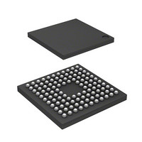
IC H8S/2214 MCU FLASH 112-TFBGA
Manufacturer
Renesas Electronics America
Series
H8® H8S/2200r
Datasheets
1.HS2214ECB62H.pdf
(938 pages)
2.HEWH8E10A.pdf
(19 pages)
3.D12312SVTE25V.pdf
(341 pages)
Specifications of DF2214BQ16V
Core Processor
H8S/2000
Core Size
16-Bit
Speed
16MHz
Connectivity
SCI
Peripherals
DMA, POR, PWM, WDT
Number Of I /o
72
Program Memory Size
128KB (128K x 8)
Program Memory Type
FLASH
Ram Size
12K x 8
Voltage - Supply (vcc/vdd)
2.7 V ~ 3.6 V
Data Converters
D/A 1x8b
Oscillator Type
Internal
Operating Temperature
-20°C ~ 75°C
Package / Case
112-TFBGA
For Use With
HS0005KCU11H - EMULATOR E10A-USB H8S(X),SH2(A)3DK2218 - DEV EVAL KIT H8S/2218
Lead Free Status / RoHS Status
Lead free / RoHS Compliant
Eeprom Size
-
Available stocks
Company
Part Number
Manufacturer
Quantity
Price
Company:

Part Number:
DF2214BQ16V
Manufacturer:
Renesas Electronics America
Quantity:
10 000


Figure 8.6
Figure 8.7
Figure 8.8
Figure 8.9
Figure 8.10 DTC Operation Timing (Example in Normal Mode or Repeat Mode) ................... 274
Figure 8.11 DTC Operation Timing
Figure 8.12 DTC Operation Timing (Example of Chain Transfer) ............................................ 275
Section 9 I/O Ports
Figure 9.1
Figure 9.2
Figure 9.3
Figure 9.4
Figure 9.5
Figure 9.6
Figure 9.7
Figure 9.8
Figure 9.9
Figure 9.10 Port C Pin Functions (Mode 6)................................................................................ 334
Figure 9.11 Port C Pin Functions (Mode 7)................................................................................ 335
Figure 9.12 Port D Pin Functions ............................................................................................... 337
Figure 9.13 Port D Pin Functions (Modes 4 to 6)....................................................................... 340
Figure 9.14 Port D Pin Functions (Mode 7) ............................................................................... 341
Figure 9.15 Port E Pin Functions................................................................................................ 342
Figure 9.16 Port E Pin Functions (Modes 4 to 6) ....................................................................... 345
Figure 9.17 Port E Pin Functions (Mode 7)................................................................................ 346
Figure 9.18 Port F Pin Functions................................................................................................ 348
Figure 9.19 Port G Pin Functions ............................................................................................... 353
Section 10 16-Bit Timer Pulse Unit (TPU)
Figure 10.1 Block Diagram of TPU ........................................................................................... 363
Figure 10.2 16-Bit Register Access Operation [Bus Master ↔ TCNT (16 Bits)] ...................... 389
Figure 10.3 8-Bit Register Access Operation [Bus Master ↔ TCR (Upper 8 Bits)].................. 390
Figure 10.4 8-Bit Register Access Operation [Bus Master ↔ TMDR (Lower 8 Bits)] ............. 390
Figure 10.5 8-Bit Register Access Operation [Bus Master ↔ TCR and TMDR (16 Bits)] ....... 390
Figure 10.6 Example of Counter Operation Setting Procedure .................................................. 392
Figure 10.7 Free-Running Counter Operation ............................................................................ 393
Figure 10.8 Periodic Counter Operation..................................................................................... 394
Figure 10.9 Example Of Setting Procedure For Waveform Output By Compare Match ........... 395
Figure 10.10 Example of 0 Output/1 Output Operation ............................................................... 396
Rev.4.00 Sep. 18, 2008 Page xlviii of lx
REJ09B0189-0400
Memory Mapping in Normal Mode ........................................................................ 269
Memory Mapping in Repeat Mode ......................................................................... 270
Memory Mapping in Block Transfer Mode ............................................................ 272
Chain Transfer Memory Map.................................................................................. 273
(Example of Block Transfer Mode, with Block Size of 2)...................................... 274
Port 1 Pin Functions ................................................................................................ 285
Port 3 Pin Functions ................................................................................................ 296
Port 4 Pin Functions ................................................................................................ 304
Port 7 Pin Functions ................................................................................................ 308
Port 9 Pin Functions ................................................................................................ 314
Port A Pin Functions ............................................................................................... 315
Port B Pin Functions ............................................................................................... 322
Port C Pin Functions ............................................................................................... 330
Port C Pin Functions (Modes 4 and 5) .................................................................... 333
Related parts for DF2214BQ16V
Image
Part Number
Description
Manufacturer
Datasheet
Request
R

Part Number:
Description:
CONN SOCKET 2POS 7.92MM WHITE
Manufacturer:
Hirose Electric Co Ltd
Datasheet:

Part Number:
Description:
CONN SOCKET 4POS 7.92MM WHITE
Manufacturer:
Hirose Electric Co Ltd
Datasheet:

Part Number:
Description:
CONN SOCKET 5POS 7.92MM WHITE
Manufacturer:
Hirose Electric Co Ltd
Datasheet:

Part Number:
Description:
CONN SOCKET 3POS 7.92MM WHITE
Manufacturer:
Hirose Electric Co Ltd
Datasheet:
Part Number:
Description:
CONN SOCKET 5POS 7.92MM WHITE
Manufacturer:
Hirose Electric Co Ltd
Datasheet:

Part Number:
Description:
CONN SOCKET 2POS 7.92MM WHITE
Manufacturer:
Hirose Electric Co Ltd
Datasheet:
Part Number:
Description:
CONN SOCKET 3POS 7.92MM WHITE
Manufacturer:
Hirose Electric Co Ltd
Datasheet:
Part Number:
Description:
CONN SOCKET 4POS 7.92MM WHITE
Manufacturer:
Hirose Electric Co Ltd
Datasheet:

Part Number:
Description:
CONN HEADER 2POS 7.92MM R/A TIN
Manufacturer:
Hirose Electric Co Ltd
Datasheet:

Part Number:
Description:
CONN HEADER 4POS 7.92MM R/A TIN
Manufacturer:
Hirose Electric Co Ltd
Datasheet:

Part Number:
Description:
KIT STARTER FOR M16C/29
Manufacturer:
Renesas Electronics America
Datasheet:

Part Number:
Description:
KIT STARTER FOR R8C/2D
Manufacturer:
Renesas Electronics America
Datasheet:

Part Number:
Description:
R0K33062P STARTER KIT
Manufacturer:
Renesas Electronics America
Datasheet:

Part Number:
Description:
KIT STARTER FOR R8C/23 E8A
Manufacturer:
Renesas Electronics America
Datasheet:

Part Number:
Description:
KIT STARTER FOR R8C/25
Manufacturer:
Renesas Electronics America
Datasheet: