DF2214BQ16V Renesas Electronics America, DF2214BQ16V Datasheet - Page 34
DF2214BQ16V
Manufacturer Part Number
DF2214BQ16V
Description
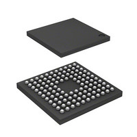
IC H8S/2214 MCU FLASH 112-TFBGA
Manufacturer
Renesas Electronics America
Series
H8® H8S/2200r
Datasheets
1.HS2214ECB62H.pdf
(938 pages)
2.HEWH8E10A.pdf
(19 pages)
3.D12312SVTE25V.pdf
(341 pages)
Specifications of DF2214BQ16V
Core Processor
H8S/2000
Core Size
16-Bit
Speed
16MHz
Connectivity
SCI
Peripherals
DMA, POR, PWM, WDT
Number Of I /o
72
Program Memory Size
128KB (128K x 8)
Program Memory Type
FLASH
Ram Size
12K x 8
Voltage - Supply (vcc/vdd)
2.7 V ~ 3.6 V
Data Converters
D/A 1x8b
Oscillator Type
Internal
Operating Temperature
-20°C ~ 75°C
Package / Case
112-TFBGA
For Use With
HS0005KCU11H - EMULATOR E10A-USB H8S(X),SH2(A)3DK2218 - DEV EVAL KIT H8S/2218
Lead Free Status / RoHS Status
Lead free / RoHS Compliant
Eeprom Size
-
Available stocks
Company
Part Number
Manufacturer
Quantity
Price
Company:

Part Number:
DF2214BQ16V
Manufacturer:
Renesas Electronics America
Quantity:
10 000


2.9
2.10 Usage Notes ......................................................................................................................... 65
Section 3 MCU Operating Modes .......................................................................71
3.1
3.2
3.3
3.4
3.5
Section 4 Exception Handling .............................................................................79
4.1
4.2
4.3
Rev.4.00 Sep. 18, 2008 Page xxxii of lx
REJ09B0189-0400
2.8.4
2.8.5
2.8.6
Basic Timing........................................................................................................................ 62
2.9.1
2.9.2
2.9.3
2.9.4
2.10.1 TAS Instruction....................................................................................................... 65
2.10.2 STM/LDM Instruction Usage ................................................................................. 66
2.10.3 Bit Manipulation Instructions ................................................................................. 66
2.10.4 Access Methods for Registers with Write-Only Bits .............................................. 68
Overview.............................................................................................................................. 71
3.1.1
3.1.2
Register Descriptions ........................................................................................................... 72
3.2.1
3.2.2
Operating Mode Descriptions .............................................................................................. 75
3.3.1
3.3.2
3.3.3
3.3.4
Pin Functions in Each Operating Mode ............................................................................... 77
Memory Map in Each Operating Mode ............................................................................... 77
Overview.............................................................................................................................. 79
4.1.1
4.1.2
4.1.3
Reset
4.2.1
4.2.2
4.2.3
4.2.4
4.2.5
Traces ................................................................................................................................ 86
Program Execution State......................................................................................... 61
Bus-Released State ................................................................................................. 61
Power-Down State .................................................................................................. 61
Overview................................................................................................................. 62
On-Chip Memory (ROM, RAM) ............................................................................ 62
On-Chip Supporting Module Access Timing ......................................................... 64
External Address Space Access Timing ................................................................. 65
Operating Mode Selection ...................................................................................... 71
Register Configuration............................................................................................ 72
Mode Control Register (MDCR) ............................................................................ 72
System Control Register (SYSCR) ......................................................................... 73
Mode 4 .................................................................................................................... 75
Mode 5 .................................................................................................................... 75
Mode 6 .................................................................................................................... 76
Mode 7 .................................................................................................................... 76
Exception Handling Types and Priority.................................................................. 79
Exception Handling Operation................................................................................ 80
Exception Sources and Vector Table ...................................................................... 80
Overview................................................................................................................. 82
Reset Types............................................................................................................. 82
Reset Sequence ....................................................................................................... 83
Interrupts after Reset............................................................................................... 85
State of On-Chip Supporting Modules after Reset Release .................................... 85
................................................................................................................................ 82
Related parts for DF2214BQ16V
Image
Part Number
Description
Manufacturer
Datasheet
Request
R

Part Number:
Description:
CONN SOCKET 2POS 7.92MM WHITE
Manufacturer:
Hirose Electric Co Ltd
Datasheet:

Part Number:
Description:
CONN SOCKET 4POS 7.92MM WHITE
Manufacturer:
Hirose Electric Co Ltd
Datasheet:

Part Number:
Description:
CONN SOCKET 5POS 7.92MM WHITE
Manufacturer:
Hirose Electric Co Ltd
Datasheet:

Part Number:
Description:
CONN SOCKET 3POS 7.92MM WHITE
Manufacturer:
Hirose Electric Co Ltd
Datasheet:
Part Number:
Description:
CONN SOCKET 5POS 7.92MM WHITE
Manufacturer:
Hirose Electric Co Ltd
Datasheet:

Part Number:
Description:
CONN SOCKET 2POS 7.92MM WHITE
Manufacturer:
Hirose Electric Co Ltd
Datasheet:
Part Number:
Description:
CONN SOCKET 3POS 7.92MM WHITE
Manufacturer:
Hirose Electric Co Ltd
Datasheet:
Part Number:
Description:
CONN SOCKET 4POS 7.92MM WHITE
Manufacturer:
Hirose Electric Co Ltd
Datasheet:

Part Number:
Description:
CONN HEADER 2POS 7.92MM R/A TIN
Manufacturer:
Hirose Electric Co Ltd
Datasheet:

Part Number:
Description:
CONN HEADER 4POS 7.92MM R/A TIN
Manufacturer:
Hirose Electric Co Ltd
Datasheet:

Part Number:
Description:
KIT STARTER FOR M16C/29
Manufacturer:
Renesas Electronics America
Datasheet:

Part Number:
Description:
KIT STARTER FOR R8C/2D
Manufacturer:
Renesas Electronics America
Datasheet:

Part Number:
Description:
R0K33062P STARTER KIT
Manufacturer:
Renesas Electronics America
Datasheet:

Part Number:
Description:
KIT STARTER FOR R8C/23 E8A
Manufacturer:
Renesas Electronics America
Datasheet:

Part Number:
Description:
KIT STARTER FOR R8C/25
Manufacturer:
Renesas Electronics America
Datasheet: