DF2214BQ16V Renesas Electronics America, DF2214BQ16V Datasheet - Page 41
DF2214BQ16V
Manufacturer Part Number
DF2214BQ16V
Description
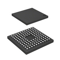
IC H8S/2214 MCU FLASH 112-TFBGA
Manufacturer
Renesas Electronics America
Series
H8® H8S/2200r
Datasheets
1.HS2214ECB62H.pdf
(938 pages)
2.HEWH8E10A.pdf
(19 pages)
3.D12312SVTE25V.pdf
(341 pages)
Specifications of DF2214BQ16V
Core Processor
H8S/2000
Core Size
16-Bit
Speed
16MHz
Connectivity
SCI
Peripherals
DMA, POR, PWM, WDT
Number Of I /o
72
Program Memory Size
128KB (128K x 8)
Program Memory Type
FLASH
Ram Size
12K x 8
Voltage - Supply (vcc/vdd)
2.7 V ~ 3.6 V
Data Converters
D/A 1x8b
Oscillator Type
Internal
Operating Temperature
-20°C ~ 75°C
Package / Case
112-TFBGA
For Use With
HS0005KCU11H - EMULATOR E10A-USB H8S(X),SH2(A)3DK2218 - DEV EVAL KIT H8S/2218
Lead Free Status / RoHS Status
Lead free / RoHS Compliant
Eeprom Size
-
Available stocks
Company
Part Number
Manufacturer
Quantity
Price
Company:

Part Number:
DF2214BQ16V
Manufacturer:
Renesas Electronics America
Quantity:
10 000


10.5 Interrupts ............................................................................................................................ 416
10.6 Operation Timing............................................................................................................... 418
10.7 Usage Notes ....................................................................................................................... 427
Section 11 Watchdog Timer (WDT)................................................................. 437
11.1 Overview............................................................................................................................ 437
11.2 Register Descriptions ......................................................................................................... 440
11.3 Operation............................................................................................................................ 446
11.4 Interrupts ............................................................................................................................ 449
11.5 Usage Notes ....................................................................................................................... 450
Section 12 Serial Communication Interface (SCI) ........................................... 453
12.1 Overview............................................................................................................................ 453
10.4.1 Overview............................................................................................................... 391
10.4.2 Basic Functions..................................................................................................... 392
10.4.3 Synchronous Operation......................................................................................... 399
10.4.4 Buffer Operation ................................................................................................... 401
10.4.5 PWM Modes ......................................................................................................... 405
10.4.6 Phase Counting Mode ........................................................................................... 411
10.5.1 Interrupt Sources and Priorities............................................................................. 416
10.5.2 DTC and DMAC Activation ................................................................................. 417
10.6.1 Input/Output Timing ............................................................................................. 418
10.6.2 Interrupt Signal Timing......................................................................................... 423
11.1.1 Features................................................................................................................. 437
11.1.2 Block Diagram ...................................................................................................... 438
11.1.3 Register Configuration.......................................................................................... 439
11.2.1 Timer Counter (TCNT)......................................................................................... 440
11.2.2 Timer Control/Status Register (TCSR) ................................................................. 440
11.2.3 Reset Control/Status Register (RSTCSR) ............................................................. 442
11.2.4 Notes on Register Access...................................................................................... 444
11.3.1 Watchdog Timer Operation .................................................................................. 446
11.3.2 Interval Timer Operation ...................................................................................... 447
11.3.3 Timing of Setting of Overflow Flag (OVF) .......................................................... 448
11.3.4 Timing of Setting of Watchdog Timer Overflow Flag (WOVF) .......................... 449
11.5.1 Contention between Timer Counter (TCNT) Write and Increment ...................... 450
11.5.2 Changing Value of CKS2 to CKS0....................................................................... 450
11.5.3 Switching between Watchdog Timer Mode and Interval Timer Mode................. 451
11.5.4 Internal Reset in Watchdog Timer Mode.............................................................. 451
11.5.5 OVF Flag Clear Operation in Interval Timer Mode.............................................. 451
12.1.1 Features................................................................................................................. 453
12.1.2 Block Diagram ...................................................................................................... 455
Rev.4.00 Sep. 18, 2008 Page xxxix of lx
REJ09B0189-0400
Related parts for DF2214BQ16V
Image
Part Number
Description
Manufacturer
Datasheet
Request
R

Part Number:
Description:
CONN SOCKET 2POS 7.92MM WHITE
Manufacturer:
Hirose Electric Co Ltd
Datasheet:

Part Number:
Description:
CONN SOCKET 4POS 7.92MM WHITE
Manufacturer:
Hirose Electric Co Ltd
Datasheet:

Part Number:
Description:
CONN SOCKET 5POS 7.92MM WHITE
Manufacturer:
Hirose Electric Co Ltd
Datasheet:

Part Number:
Description:
CONN SOCKET 3POS 7.92MM WHITE
Manufacturer:
Hirose Electric Co Ltd
Datasheet:
Part Number:
Description:
CONN SOCKET 5POS 7.92MM WHITE
Manufacturer:
Hirose Electric Co Ltd
Datasheet:

Part Number:
Description:
CONN SOCKET 2POS 7.92MM WHITE
Manufacturer:
Hirose Electric Co Ltd
Datasheet:
Part Number:
Description:
CONN SOCKET 3POS 7.92MM WHITE
Manufacturer:
Hirose Electric Co Ltd
Datasheet:
Part Number:
Description:
CONN SOCKET 4POS 7.92MM WHITE
Manufacturer:
Hirose Electric Co Ltd
Datasheet:

Part Number:
Description:
CONN HEADER 2POS 7.92MM R/A TIN
Manufacturer:
Hirose Electric Co Ltd
Datasheet:

Part Number:
Description:
CONN HEADER 4POS 7.92MM R/A TIN
Manufacturer:
Hirose Electric Co Ltd
Datasheet:

Part Number:
Description:
KIT STARTER FOR M16C/29
Manufacturer:
Renesas Electronics America
Datasheet:

Part Number:
Description:
KIT STARTER FOR R8C/2D
Manufacturer:
Renesas Electronics America
Datasheet:

Part Number:
Description:
R0K33062P STARTER KIT
Manufacturer:
Renesas Electronics America
Datasheet:

Part Number:
Description:
KIT STARTER FOR R8C/23 E8A
Manufacturer:
Renesas Electronics America
Datasheet:

Part Number:
Description:
KIT STARTER FOR R8C/25
Manufacturer:
Renesas Electronics America
Datasheet: