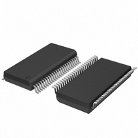
SC28L201A1DGG,118 NXP Semiconductors, SC28L201A1DGG,118 Datasheet - Page 95

SC28L201A1DGG,118
Manufacturer Part Number
SC28L201A1DGG,118
Description
IC UART W/FIFO 48-TSSOP
Manufacturer
NXP Semiconductors
Series
IMPACTr
Datasheet
1.SC28L201A1DGG118.pdf
(110 pages)
Specifications of SC28L201A1DGG,118
Features
False-start Bit Detection
Number Of Channels
2, DUART
Fifo's
256 Byte
Voltage - Supply
3.3V, 5V
With Parallel Port
Yes
With Auto Flow Control
Yes
With False Start Bit Detection
Yes
With Modem Control
Yes
With Cmos
Yes
Mounting Type
Surface Mount
Package / Case
48-TSSOP
Lead Free Status / RoHS Status
Lead free / RoHS Compliant
Other names
935277824118
SC28L201A1DGG-T
SC28L201A1DGG-T
SC28L201A1DGG-T
SC28L201A1DGG-T
Philips Semiconductors
Table 82:
T
[1]
[2]
[3]
[4]
[5]
[6]
[7]
9397 750 13138
Product data sheet
Symbol
t
t
t
t
t
t
t
t
t
h(D)(mot)
su(An-CENL)(mot)
h(CENL-An)(mot)
Dv(CENL)
d(RWD)(mot)
DCR
DCW
DAT
CSC
amb
Test conditions for outputs: C
Timing is illustrated and referenced to the WRN and RDN inputs. Also, CEN may be the ‘strobing’ input. CEN and RDN (also CEN and
WRN) are ORed internally. The signal asserted last initiates the cycle and the signal negated first terminates the cycle.
Guaranteed by characterization of sample units.
If CEN is used as the ‘strobing’ input, the parameter defines the minimum HIGH times between one CEN and the next. The RDN signal
must be negated for t
Minimum frequencies are not tested, but are guaranteed by design.
Clocks for 1 mode should be reasonably symmetrical.
Data is usually setup with respect to CEN going LOW (the leading edge of CEN). This mode strongly implies the use of DACKN. (Its use
is not strictly required.) DACKN is derived from the X1/SCLK input. It is seldom that the system clocks that ultimately drive the CEN,
address, and R/WN signals are synchronous to the X1/SCLK. If address, data, R/WN are setup before CEN goes LOW and hold
through DACKN, the timing parameters above will be guaranteed.
= 40 C to +85 C; voltage tolerance
Dynamic characteristics
Parameter
CEN HIGH to data hold time
address to CEN LOW setup
time
CEN LOW to address hold time
CEN LOW to data valid time
read and write cycle HIGH time
X1/SCLK HIGH to DACKN LOW
time (read cycle)
X1/SCLK HIGH to DACKN LOW
time (write cycle)
CEN to IACKN HIGH DACKN
high-impedance time
CEN or IACKN to X1/SCLK
HIGH setup time
d(RWD)
time to guarantee that any Status Register changes are valid.
L
= 85 pF, except interrupt outputs. Test conditions for interrupt outputs: C
…continued
10 %; unless otherwise specified.
Rev. 01 — 31 October 2005
Conditions
for minimum DACKN cycle
3.3 V, 5 V UART, 3.125 Mbit/s, with 256-byte FIFO
[1]
[2] [4]
V
Min
© Koninklijke Philips Electronics N.V. 2005. All rights reserved.
10
10
10
10
DD
0
-
-
-
-
= 3.3 V
L
Max
= 85 pF, R
45
35
30
15
-
-
-
-
-
SC28L201
Min
10
10
10
10
V
0
L
-
-
-
-
DD
= 2.7 k to V
= 5 V
Max
35
35
25
15
-
-
-
-
-
95 of 110
Unit
ns
ns
ns
ns
ns
ns
ns
ns
ns
DD
.


