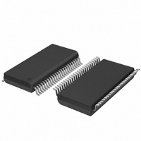
SC28L201A1DGG,118 NXP Semiconductors, SC28L201A1DGG,118 Datasheet - Page 25

SC28L201A1DGG,118
Manufacturer Part Number
SC28L201A1DGG,118
Description
IC UART W/FIFO 48-TSSOP
Manufacturer
NXP Semiconductors
Series
IMPACTr
Datasheet
1.SC28L201A1DGG118.pdf
(110 pages)
Specifications of SC28L201A1DGG,118
Features
False-start Bit Detection
Number Of Channels
2, DUART
Fifo's
256 Byte
Voltage - Supply
3.3V, 5V
With Parallel Port
Yes
With Auto Flow Control
Yes
With False Start Bit Detection
Yes
With Modem Control
Yes
With Cmos
Yes
Mounting Type
Surface Mount
Package / Case
48-TSSOP
Lead Free Status / RoHS Status
Lead free / RoHS Compliant
Other names
935277824118
SC28L201A1DGG-T
SC28L201A1DGG-T
SC28L201A1DGG-T
SC28L201A1DGG-T
Philips Semiconductors
9397 750 13138
Product data sheet
will enable itself to receive the following data stream. Upon receipt of an address not its
own it would then disable itself. As described below appropriate status bits are available to
describe the operation. Again, for this mode an ‘address byte’ is a byte that has the bit in
the parity position set to logical 1.
The use of the multi-drop mode usually implies a ‘master and slave’ configuration, but is
not required, of the several UART stations so programmed. The software control should
allow time for the slave stations to respond to the receipt of an address bit. Often a reply
from the addressed station is expected to confirm the receipt of the address. Please see
Section 8.2.4 “Mode Register 3
Enabling the Wake-up mode:
‘multi-drop’.)
This mode is selected by programming bits MR1[4:3] (the parity bits) to ‘11’. The wake-up
feature has four modes of operation: one strictly under processor control and three
automatic. These modes are controlled by bits 6, 1, 0 in the MR3 register. Bit 6 controls
the loading of the address byte to the RxFIFO and MR3[1:0] determines the sub-mode as
shown in the following list.
MR3[1:0] = 00 Normal Wake-up Mode (default), which is the same as previous UARTs,
and is therefore under full control of the processor. The Host controls operation via
interrupts it receives and commands it writes to the UART Command Registers (CR).
Normal wake-up (the default configuration):
executes a partial enabling of the receiver state machine. Even though the receiver has
been reset, the Wake-up mode will override the disable and reset condition.
In the default (mode ‘00’ above and the least efficient) configuration for this mode of
operation, a ‘master’ station transmits an address character followed by data characters
for the addressed ‘slave’ station. The slave stations, whose receivers are normally
disabled (not reset), examine the received data stream. Upon recognition of its address bit
(this is the parity bit redefined to indicate the associated byte is an address byte,
not the address itself) interrupts the CPU (by setting RxRDY). The CPU (host) compares
the received address to its station address and enables the receiver if it wishes to receive
the subsequent data characters. Upon receipt of another address character, the CPU may
disable the receiver to initiate the process again.
A transmitted character consists of a start bit; the programmed number of data bits, an
address/data (A/D) bit and the programmed number of stop bits. The CPU selects the
polarity of the transmitted A/D bit by programming bit MR1[2]. MR1[2] = 0 transmits a zero
in the A/D bit position which identifies the corresponding data bits as data. MR1 [2] = 1
transmits a one in the A/D bit position which identifies the corresponding data bits as an
address. The CPU should program the mode register prior to loading the corresponding
data bytes into the TxFIFO.
While in this mode, the receiver continuously looks at the received data stream, whether it
is enabled or disabled. If disabled, it sets the RxRDY status bit and loads the character
into the RxFIFO if the received A/D bit is a one, but discards the received character if the
received A/D bit is a zero. If the receiver is enabled, all received characters are transferred
to the CPU via the RxFIFO. In either case when the address character is recognized the
data bits are loaded into the data FIFO while the A/D bit is loaded into the status FIFO
position normally used for parity error (SR[5]). Framing error, overrun error, and break
Rev. 01 — 31 October 2005
(This mode is variously referred to as ‘9-bit’ or
(MR3)”.
3.3 V, 5 V UART, 3.125 Mbit/s, with 256-byte FIFO
The enabling of the Wake-up mode
© Koninklijke Philips Electronics N.V. 2005. All rights reserved.
SC28L201
25 of 110


