SC28L201A1DGG,118 NXP Semiconductors, SC28L201A1DGG,118 Datasheet
SC28L201A1DGG,118
Specifications of SC28L201A1DGG,118
SC28L201A1DGG-T
SC28L201A1DGG-T


Related parts for SC28L201A1DGG,118


SC28L201A1DGG,118 Summary of contents
Page 1
SC28L201 3 UART, 3.125 Mbit/s, with 256-byte FIFO Rev. 01 — 31 October 2005 1. General description The SC28L201 is a high performance UART. Its functional and programming features closely match but greatly extend those of previous ...
Page 2
Philips Semiconductors 2. Features Member of IMPACT family +85 C and 80xxx or 68000 bus interface (I/M modes) Bit-by-bit real time transmission error check for high data integrity systems Full-duplex independent asynchronous ...
Page 3
Philips Semiconductors Automatic Wake-up mode for multi-drop applications Start-end break interrupt/status Detects break which originates in the middle of a character On-chip crystal oscillator Power-down mode at less than 10 A Receiver Time-out mode Single +3 Ordering information ...
Page 4
Philips Semiconductors 4. Block diagram RDN WRN CEN RESET IRQN X1/SCLK X2 Fig 1. Block diagram of SC28L201 (80xxx mode) 9397 750 13138 Product data sheet 3 UART, 3.125 Mbit/s, with ...
Page 5
Philips Semiconductors R/WN IACKN CEN RESETN IRQN DACKN X1/SCLK X2 Fig 2. Block diagram of SC28L201 (68000 mode) 9397 750 13138 Product data sheet 3 UART, 3.125 Mbit/s, with 256-byte FIFO ...
Page 6
Philips Semiconductors 5. Pinning information 5.1 Pinning RXD 7 8 RESET SC28L201A1DGG 80xxx mode V ...
Page 7
Philips Semiconductors Table 2: Pin description for 80xxx bus interface (Intel) See Figure 3. Symbol Pin Type RDN 20, 21, 22 RESET 8 I IRQN 46 O IACKN 23 I ...
Page 8
Philips Semiconductors Table 3: Pin description for 68000 bus interface (Motorola) See Figure 4. Symbol Pin Type MODE_IM 18, 17, 16, I/O 15, 12, 11, 10, 9 CEN IACKN 23 ...
Page 9
Philips Semiconductors Table 3: Pin description for 68000 bus interface (Motorola) See Figure 4. Symbol Pin Type I/O6B 29 I/O I/O4B to I/O2B 30, 31, 32 I/O0B 13, 24, power 14, 25, power ...
Page 10
Philips Semiconductors 6.1.2 Timing circuits 6.1.2.1 Crystal oscillator The crystal oscillator is the main timing element for the SC28L201 nominally set at 14.7456 MHz. Operation with a crystal as a frequency standard is specified from 7 MHz to ...
Page 11
Philips Semiconductors 6.1.4 UART The UART is a fully independent, full duplex and provides all normal asynchronous functions data bits, parity odd or even, programmable stop bit length, false start bit detection. Also provided are 256-byte FIFOs, ...
Page 12
Philips Semiconductors The content of the current interrupt register also drives the Global Registers of the interrupt system. These registers are indirect addresses (pointers) to the interrupt source requesting service. Programming of Bid Control Registers allows the interrupt level of ...
Page 13
Philips Semiconductors 7. Detailed descriptions Remark: For the convenience of the reader, some paragraphs of the following sections are repeated in descriptions of closely linked functions described in other sections. 7.1 Bus interface The bus interface operates in two modes ...
Page 14
Philips Semiconductors When operating in the 86xxx mode, DACKN is not generated. Data is written on the termination of CEN or WRN, whichever one occurs first. Read data is presented from the leading edge of the read condition (CEN and ...
Page 15
Philips Semiconductors 7.2 Timing circuits 7.2.1 Crystal oscillator The crystal oscillator operates directly from a crystal, tuned between 7.0 MHz and 16.2 MHz connected across the X1/SCLK and X2 inputs with a minimum of external components. BRG values listed for ...
Page 16
Philips Semiconductors RXFIFO that has not been read. The Counter/Timer uses the numbers loaded into the Counter/Timer Lower Register (CTPL and the Counter/Timer Upper Register (CTPU) as its divisor. The counter/timer is controlled with six commands: Start/Stop C/T, Read/Write Counter/Timer ...
Page 17
Philips Semiconductors Each timer unit has eight different clock sources available to it, as described in 8.4.6 “Programmable BRG Clock Source, 0 and 1 stop controls are also contained in this register. The PBRG counters generate a symmetrical square wave ...
Page 18
Philips Semiconductors When legacy code is called using the lower 16 address portions (0x00 to 0x0F), the I/O pins will be switched to input. Legacy code would expect to see the I/OA pins to be input and the I/OB pins ...
Page 19
Philips Semiconductors transmitter enable/disable bit in the command register is at zero the TxFIFO will not accept any more characters and the Tx Idle and TxRDY bits of the status register set to zero. 7.4.3 Transmission of ‘break’ Transmission of ...
Page 20
Philips Semiconductors The TxRDY bit is set whenever the transmitter is enabled and the TxFIFO is not full. Data is transferred from the holding register to Transmit Shift Register when it is idle or has completed transmission of the previous ...
Page 21
Philips Semiconductors 7.4.7.1 1x and 16x modes, receiver The receiver operates in one of two modes: 1 and the two, the far more robust and the preferred mode. Although the 1 mode may allow ...
Page 22
Philips Semiconductors 7.4.7.3 Receiver status bits There are five (5) status bits that are evaluated with each byte (or character) received: received break, framing error, parity error, overrun error, and change of break. The first three are appended to each ...
Page 23
Philips Semiconductors The ‘change of break’ means that either a break has been detected or that the break condition has been cleared. This bit is available in the ISR. The break change bit being set in the ISR and the ...
Page 24
Philips Semiconductors with a ‘receiver reset’ issued from the Command Register or a chip reset is issued. The purpose of this mode is indicating an error in the data block as opposed to an error in a character. This mode ...
Page 25
Philips Semiconductors will enable itself to receive the following data stream. Upon receipt of an address not its own it would then disable itself. As described below appropriate status bits are available to describe the operation. Again, for this mode ...
Page 26
Philips Semiconductors detect operate normally whether or not the receiver is enabled. When the automatic modes are in operation the loading of the address character to the FIFO is controlled by the MR0[6] bit. The several automatic controls. These modes ...
Page 27
Philips Semiconductors 7.4.7.9 Receiver Time-out mode Remark: This is similar to the watchdog above, but its more precise meaning is that the receiver data stream has stopped. In addition to the watchdog timer described in used for a similar function. ...
Page 28
Philips Semiconductors updated by an arbitration or bidding unit that selects the highest value presented by the various interrupt sources that may be enabled at any time. The values used are under the control of the software and the FIFO ...
Page 29
Philips Semiconductors Associated with the interrupt system are the Interrupt Mask Register (IMR) and the Interrupt Status Register (ISR) resident in each UART. Programming of the IMR selects which of the above sources may enter the arbitration process. The IMR ...
Page 30
Philips Semiconductors Table 4: Interrupt values Type Bit 11 to bit 4 receiver without error RxFIFO filled Byte Count receiver with error RxFIFO filled Byte Count receiver watchdog RxFIFO filled Byte Count transmitter TxFIFO empty Byte Count change of break ...
Page 31
Philips Semiconductors For example: The break condition is sometimes used to signal a starting point in a continuous stream of data. A Continuous running weather report or stock market ‘ticker-tape’ report needs breaks in the data so that a receiver ...
Page 32
Philips Semiconductors • GTxFIFO: pointer to the interrupting transmitter FIFO A read of the GRxFIFO will give the content of the RxFIFO that presently has the highest bid value. The purpose of this system is to enhance the efficiency of ...
Page 33
Philips Semiconductors Remark: Reading the XISR Clears the status bits associated with the recognition. The characters of the recognition system are fully programmable. The Xon/Xoff characters will be set to the standard characters if the hardware or software reset is ...
Page 34
Philips Semiconductors 11 — Auto Rx and Tx control. Receiver commands Tx to send Xoff as the receiver fills and commands the Tx to send Xon when Rx FIFO fill level is lowered. This results in total automatic control. No ...
Page 35
Philips Semiconductors 7.4.10.5 Receiver mode Since the receiving FIFO resources in the UART are limited, some means of controlling a remote transmitter is desirable in order to lessen the probability of receiver overrun. The UART provides two methods of controlling ...
Page 36
Philips Semiconductors 7.4.10.7 Xon/Xoff interrupts The Xon/Xoff logic generates interrupts only in response to recognizing either of the characters in the XonCR or XoffCR (Xon or Xoff Character Registers). The transmitter activity initiated by the Xon/Xoff logic or any CR ...
Page 37
Philips Semiconductors Writing control words into the appropriate registers programs the operation of the UART. Operational feedback is provided via status registers that can be read by the CPU. The addressing of the registers is described in The contents of ...
Page 38
Philips Semiconductors Table 5: Bit 2:1 0 Table 6: X1/SCLK 3.6864 MHz 7.3728 MHz 14.7456 MHz 29.4912 MHz 33.1776 MHz 44.2368 MHz 9397 750 13138 Product data sheet GCCR - Global Configuration Control Register (address 0x66) bit description Symbol Description ...
Page 39
Philips Semiconductors 8.1.2 Special Feature and Status Register (SFSR A and B) Table 7: Bit 7:4 3 2:1 0 8.1.3 Test and Revision Register (TRR) Table 8: Bit 7 6:0 9397 750 13138 Product data sheet 3 ...
Page 40
Philips Semiconductors 8.1.4 Scan Test Control Register (STCR) Table 9: Bit 7 8.1.5 System Enable Status register A and B (SES) This register reports the enabled status of the several sub-systems in the UART. These systems are ...
Page 41
Philips Semiconductors 8.1.6 Enhanced Operation Status register (EOS) This register reports the status of the Enhanced operation in several sub-systems in the UART. Table 11: Bit 8.2 UART registers Remark: These registers ...
Page 42
Philips Semiconductors 8.2.1 Mode Register 0 (MR0) MR0 can be accessed directly at H’20’ and 0x20 in the Extended section of the address map means of the ‘MR Pointers’ at the 0x00 used by legacy code. Table 12: ...
Page 43
Philips Semiconductors Table 13: MR0[ Table 14: MR0[ Table 15: MR0[ Table 16: MR0[ 9397 750 13138 Product data sheet 3 ...
Page 44
Philips Semiconductors 8.2.2 Mode Register 1 (MR1) MR1 can be accessed directly at 0x21 in the Extended section of the address map means of the MR Pointers at 0x00 used by legacy code. Table 17: Bit 7 6 ...
Page 45
Philips Semiconductors Table 17: Bit 4:3 2 1:0 9397 750 13138 Product data sheet 3 UART, 3.125 Mbit/s, with 256-byte FIFO MR1 - Mode Register 1 (address 0x21) bit description Symbol Description Parity Mode Select 00 = ...
Page 46
Philips Semiconductors 8.2.3 Mode Register 2 (MR2) MR2 can be accessed directly at 0x22 in the Extended section of the address map means of the MR Pointer at 0x00 used by legacy code. The MR2 register provides basic ...
Page 47
Philips Semiconductors Table 18: Bit 5 4 3:0 9397 750 13138 Product data sheet MR2 - Mode Register 2 (address 0x22) bit description Symbol Description Tx Controls RTS. Transmitter Request-to-Send Control. This bit controls the deactivation of the RTSN output ...
Page 48
Philips Semiconductors 8.2.4 Mode Register 3 (MR3) Table 19: Bit 7 6 5:4 3:2 9397 750 13138 Product data sheet MR3 - Mode Register 3 (address 0x23) bit description Symbol Description Xon/Xoff transparency 0 = flow control characters received are ...
Page 49
Philips Semiconductors Table 19: Bit 1:0 [1] If this bit is not ‘0’, the characters will be stripped regardless of bits [3:2] or [1:0]. 8.2.5 Receiver Clock Select Register (RxCSR) and Transmitter Clock Select Register (TxCSR) Table 20: Bit 7:6 ...
Page 50
Philips Semiconductors Table 21: SCLK maximum rate is 50 MHz. Data clock rates will follow exactly the ratio of the X1/SCLK to 14.7456 MHz TX clock select code 00 0000 00 0001 00 0010 00 0011 00 0100 00 0101 ...
Page 51
Philips Semiconductors 8.2.6 Command Register Extension (CRx used to write commands to the UART. Table 23: Bit 9397 750 13138 Product data sheet 3 UART, 3.125 Mbit/s, with 256-byte FIFO CRx - ...
Page 52
Philips Semiconductors Table 23: Bit 4:0 9397 750 13138 Product data sheet 3 UART, 3.125 Mbit/s, with 256-byte FIFO CRx - Command Register Extension (address 0x12) bit description Symbol Description Command Register codes The encoded value of ...
Page 53
Philips Semiconductors Table 23: Bit 4:0 (cont.) 9397 750 13138 Product data sheet 3 UART, 3.125 Mbit/s, with 256-byte FIFO CRx - Command Register Extension (address 0x12) bit description Symbol Description 1 0000: Transmit an Xon character. ...
Page 54
Philips Semiconductors 8.2.7 Channel Status Register (SR) Table 24: Bit 9397 750 13138 Product data sheet SR - Channel Status Register (address 0x01) bit description Symbol Description Received Break yes ...
Page 55
Philips Semiconductors Table 24: Bit 9397 750 13138 Product data sheet SR - Channel Status Register (address 0x01) bit description Symbol Description TxRDY Transmitter Ready yes This bit, when set, indicates that ...
Page 56
Philips Semiconductors 8.2.8 Interrupt Status Register (ISR) This register provides the status of all potential interrupt sources for a UART channel. When generating an interrupt arbitration value, the contents of this register are masked by the interrupt mask register (IMR). ...
Page 57
Philips Semiconductors Table 25: Bit 1 0 9397 750 13138 Product data sheet ISR - Interrupt Status Register (address 0x25) bit description Symbol Description RxINT Receiver entered the arbitration process. (Also Rx DMA hand-shake at I/O pins.) The general function ...
Page 58
Philips Semiconductors 8.2.9 Interrupt Mask Register (IMR) The programming of this register selects which bits in the ISR cause an interrupt output bit in the ISR is a ‘1’ and the corresponding bit in the IMR is a ...
Page 59
Philips Semiconductors 8.2.10 Receiver FIFO (RxFIFO) The FIFO for the receiver is 11 bits wide and 256 words deep. The status of each byte received is stored with that byte and is moved along with the byte as the characters ...
Page 60
Philips Semiconductors 8.2.13 Receiver FIFO Fill Level register (RxFL) The number of bytes filled in the Receiver FIFO. Table 30: Bit 7:0 8.2.14 Transmitter FIFO Interrupt Level (TxFIL) The position in the Tx FIFO caused the transmitter to enter the ...
Page 61
Philips Semiconductors 8.3 Registers for character recognition Please note that, although the names of the registers imply a particular function, there is not any hardware function directly attached to them. They are just three characters that may be used for ...
Page 62
Philips Semiconductors 8.3.4 Xon/Xoff Interrupt Status Register (XISR) Reading this register clears XISR[7:4]. Table 36: Bit 7:6 5:4 3:2 1:0 9397 750 13138 Product data sheet 3 UART, 3.125 Mbit/s, with 256-byte FIFO XISR - Xon/Xoff Interrupt ...
Page 63
Philips Semiconductors 8.3.5 Watchdog, Character, Address and X Enable Register (WCXER) This register enables the UARTs Character Recognition, Address Recognition and Receiver watchdog timer. If both enable and disable are active, a disable results. This register is used to enable ...
Page 64
Philips Semiconductors 8.4 Programmable counters, timers, and baud rate generators 8.4.1 Programmable BRG Timer Reload Registers, Upper 0 and Upper 1 (PBRGPU) This is the upper byte of the 16-bit value used by the BRG timer in generating a baud ...
Page 65
Philips Semiconductors 8.4.3 Counter/Timer clock source (CTCS0 and CTCS1) Remark: Writing to this register removes the control established in the counter/timer portion of the ACR in the default register map. Table 40: Bit 7:6 5:4 3:0 9397 750 13138 Product ...
Page 66
Philips Semiconductors 8.4.4 Counter Timer Value Registers, Upper 0 and Upper 1 (CTVU0, CTVU1) Reading this register gives the value of the upper 8 bits of the Counter/Timer. Table 41: Bit 7:0 8.4.5 Counter Timer Value Registers, Lower 0 and ...
Page 67
Philips Semiconductors Table 43: Bit 3 2:0 8.4.7 Counter/Timer Preset Upper and Counter/Timer Preset Lower (CTPU, CTPL) Table 44: Bit 7:0 Table 45: Bit 7:0 The CTPU and CTPL hold the eight MSBs and eight LSBs, respectively, of the value ...
Page 68
Philips Semiconductors If the value in CTPU and CTPL is changed, the current half-period will not be affected, but subsequent half-periods will be. The C/T will not be running until it receives an initial ‘Start Counter’ command from the Command ...
Page 69
Philips Semiconductors 8.5 Registers of the Arbitrating Interrupt system and bidding control 8.5.1 Interrupt Control Register (ICR) Table 46: Bit 7:0 This register provides a single 8-bit field called the interrupt threshold for use by the interrupt arbiter. The field ...
Page 70
Philips Semiconductors 8.5.3 Current Interrupt Register (CIR) Table 48: Bit 7:6 5:1 0 The Current Interrupt Register is provided to speed up the specification of the interrupting condition in the UART. The CIR is updated at the beginning of an ...
Page 71
Philips Semiconductors Else the interrupt is another type, specified in CIR[5:1]. Remark: The GIBCR, Global Interrupting Byte Count Register, may be read to determine an exact character count. 8.5.4 Interrupt Vector Register (IVR) The IVR contains the byte that will ...
Page 72
Philips Semiconductors 8.5.7 Global Interrupting Type Register (GITR) A register associated with the interrupting channel as defined in the CIR. It contains the type of interrupt code for all interrupts. Table 52: Bit 7:6 5 4:3 2:0 8.5.8 Global RxFIFO ...
Page 73
Philips Semiconductors 8.5.10 Bidding Control Register, Break Change (BCRBRK) This register provides the 8 MSBs of the Interrupt Arbitration number for a break change interrupt. Table 55: Bit 7:0 8.5.11 Bidding Control Register, Change-Of-State (BCRCOS) This register provides the 8 ...
Page 74
Philips Semiconductors 8.6 Registers of the I/O ports 8.6.1 Input Port Change Register Lower Nibble, A (IPCRL) This register may be read to determine the current logical level of the I/O pins and examine the output of the change detectors ...
Page 75
Philips Semiconductors 8.6.2 Input Port Change Register Lower Nibble, B (IPCRL) This register may be read to determine the current logical level of the I/O pins and examine the output of the change detectors assigned to each pin. If the ...
Page 76
Philips Semiconductors 8.6.3 Input Port Change Register Upper Nibble, A (IPCRU) This register may be read to determine the current logical level of the I/O pins and examine the output of the change detectors assigned to each pin. If the ...
Page 77
Philips Semiconductors 8.6.4 Input Port Change Register Upper Nibble, B (IPCRU) This register may be read to determine the current logical level of the I/O pins and examine the output of the change detectors assigned to each pin. If the ...
Page 78
Philips Semiconductors 8.6.7 Input Change Detect Enable, A (IPCE) IPCE[7:0] bits activate the input change of state detectors pin is configured as an output, the change of state detectors, if enabled, continue to be active and will show ...
Page 79
Philips Semiconductors 8.6.8 Input Change Detect Enable, B (IPCE) IPCE[7:0] bits activate the input change of state detectors pin is configured as an output, the change of state detectors, if enabled, continue to be active and will show ...
Page 80
Philips Semiconductors Table 69: Bit 7:6 5:4 3:2 1:0 Table 70: Bit 7:6 5:4 3:2 1:0 9397 750 13138 Product data sheet 3 UART, 3.125 Mbit/s, with 256-byte FIFO I/OPCR0 - I/O Port Configuration Register (address 0x13) ...
Page 81
Philips Semiconductors Table 71: Bit 7:6 5:4 3:2 1:0 Table 72: Bit 7:6 5:4 3:2 1:0 9397 750 13138 Product data sheet 3 UART, 3.125 Mbit/s, with 256-byte FIFO I/OPCR2 - I/O Port Configuration Register (address 0x1B) ...
Page 82
Philips Semiconductors 8.6.10 Set the Output Port Bits OPR A and OPR B (SOPR A and SOPR B) Ones in the byte written to this register will cause the corresponding bit positions in the OPR to set to ‘1’. Zeros ...
Page 83
Philips Semiconductors 8.6.11 Reset Output Port bits OPR A and OPR B (ROPR A, ROPR B) Ones in the byte written to the ROPR will cause the corresponding bit positions in the OPR to set to ‘0’. Zeros have no ...
Page 84
Philips Semiconductors 8.6.12 Output Port Register A and B (OPR) The I/O pins drive the logical inverse of the data in this register. Table 75 for for B Bit ...
Page 85
Philips Semiconductors 8.7 BRG characteristics Table 76: Crystal or clock = 14.7456 MHz; duty cycle of 16 clock Normal rate (baud 110 134.5 150 200 300 600 1050 1200 1800 2000 2400 4800 7200 9600 ...
Page 86
Philips Semiconductors 9. Register maps The registers of the SC28L201 are loosely partitioned into two groups: those used in controlling data channels, and those used in handling the actual data flow and status. Below is shown the general configuration of ...
Page 87
Philips Semiconductors Table 78: Register map summary The register map for channel A (UART A). A[6:0] Read 010 0000 (0x20) Mode Register 0 (MR0 A) 010 0001 (0x21) Mode Register 1 (MR1 A) 010 0010 (0x22) Mode Register 2 (MR2 ...
Page 88
Philips Semiconductors Table 78: Register map summary The register map for channel A (UART A). A[6:0] Read 100 0000 (0x40) System Enable Status (SES A) 100 0001 (0x41) Xon Character Register (XonCR A) 100 0010 (0x42) Xoff Character Register (XoffCR ...
Page 89
Philips Semiconductors Table 78: Register map summary The register map for channel A (UART A). A[6:0] Read Global 110 0000 (0x60) Interrupt Control Register (ICR) 110 0001 (0x61) Current Interrupt Register (CIR) 110 0010 (0x62) 110 0011 (0x63) 110 0100 ...
Page 90
Philips Semiconductors 10. Limiting values Table 79: In accordance with the Absolute Maximum Rating System (IEC 60134). Symbol T amb T stg th(j-c) R th(j-a) [1] For operation at elevated temperatures, the device must ...
Page 91
Philips Semiconductors 11. Static characteristics Table 80: Static characteristics, nominal 5 V operation +85 C; unless otherwise specified. DD amb Symbol Parameter V LOW-state input voltage IL V HIGH-state ...
Page 92
Philips Semiconductors Table 81: Static characteristics, nominal 3.3 V operation +85 C; unless otherwise specified. DD amb Symbol Parameter V LOW-state input voltage IL V HIGH-state input voltage IH ...
Page 93
Philips Semiconductors 12. Dynamic characteristics Table 82: Dynamic characteristics +85 C; voltage tolerance amb Symbol Parameter Reset timing (see Figure 6 and t pulse width on pin RESET w(RESET) [2] Bus timing (see Figure 8) ...
Page 94
Philips Semiconductors Table 82: Dynamic characteristics +85 C; voltage tolerance amb Symbol Parameter Interrupt timing (see Figure 13) t interrupt delay time d(int) Clock timing (see Figure 14, Figure t X1/SCLK HIGH or LOW time ...
Page 95
Philips Semiconductors Table 82: Dynamic characteristics +85 C; voltage tolerance amb Symbol Parameter t CEN HIGH to data hold time h(D)(mot) t address to CEN LOW setup su(An-CENL)(mot) time t CEN LOW to address hold ...
Page 96
Philips Semiconductors 12.1 Timing diagrams The active time of read or write cycle exists only when CEN is LOW and RDN or CEN is also LOW. Write = CEN and WRN LOW. Read = CEN and RDN LOW. For the ...
Page 97
Philips Semiconductors CEN RDN, RWN CEN RDN, RWN CEN RDN, RWN CEN RDN, RWN a. Intel-type bus CEN R/WN (write) R/WN (read) CEN R/WN DACKN b. Motorola-type: Remark: In the 68000 mode, the write occurs on the rise of CEN ...
Page 98
Philips Semiconductors Fig 8. Bus timing (80xxx mode) Fig 9. Bus timing, read cycle (68000 mode) 9397 750 13138 Product data sheet 3 UART, 3.125 Mbit/s, with 256-byte FIFO su(An-RWL) t h(RWL-An) CEN ...
Page 99
Philips Semiconductors Fig 10. Bus timing, write cycle (68000 mode) Fig 11. Interrupt cycle timing (68000 mode) 9397 750 13138 Product data sheet 3 UART, 3.125 Mbit/s, with 256-byte FIFO t CSC X1/SCLK t su(An-RWL ...
Page 100
Philips Semiconductors a. Input pins b. Output pins Fig 12. Port timing (1) IRQN or OP3 to OP7 when used as interrupt outputs. (2) The test for open-drain outputs is intended to guarantee switching of the output transistor. Fig 13. ...
Page 101
Philips Semiconductors t CLK t CTC X1/SCLK C/T clock RxC TxC 3 pF parasitic capacitance 3 pF parasitic capacitance for C = 13.5 pF. For the oscillator feedback loop, the capacitors ...
Page 102
Philips Semiconductors D1 TXD transmitter enabled TXRDY (SR2) WRN D1 D8 (1) CTSN (IP0) (2) RTSN (OP0) OPR( (1) Timing shown for MR2[ (2) Timing shown for MR2[ Fig 17. Transmitter timing D1 RXD ...
Page 103
Philips Semiconductors master station: TXD ADD#1 transmitter enabled TXRDY (SR2) WRN MR1[4: ADD#1 MR1[ MR1[ peripheral station: bit 9 RXD 0 receiver enabled RXRDY (SR0) RDN/WRN MR1[4: Fig 19. Wake-up mode timing ...
Page 104
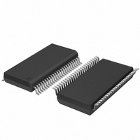
Philips Semiconductors 14. Package outline TSSOP48: plastic thin shrink small outline package; 48 leads; body width 6 pin 1 index 1 DIMENSIONS (mm are the original dimensions). A UNIT max. ...
Page 105
Philips Semiconductors 15. Soldering 15.1 Introduction to soldering surface mount packages This text gives a very brief insight to a complex technology. A more in-depth account of soldering ICs can be found in our Data Handbook IC26; Integrated Circuit Packages ...
Page 106
Philips Semiconductors – smaller than 1.27 mm, the footprint longitudinal axis must be parallel to the transport direction of the printed-circuit board. The footprint must incorporate solder thieves at the downstream end. • For packages with leads on four sides, ...
Page 107
Philips Semiconductors [4] These packages are not suitable for wave soldering. On versions with the heatsink on the bottom side, the solder cannot penetrate between the printed-circuit board and the heatsink. On versions with the heatsink on the top side, ...
Page 108
Philips Semiconductors 18. Data sheet status [1] Level Data sheet status Product status I Objective data Development II Preliminary data Qualification III Product data Production [1] Please consult the most recently issued data sheet before initiating or completing a design. ...
Page 109
Philips Semiconductors 23. Contents 1 General description . . . . . . . . . . . . . . . . . . . . . . 1 2 Features . . . . . . . . ...
Page 110
Philips Semiconductors 8.2.8 Interrupt Status Register (ISR 8.2.9 Interrupt Mask Register (IMR 8.2.10 Receiver ...