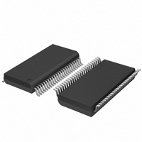
SC28L201A1DGG,118 NXP Semiconductors, SC28L201A1DGG,118 Datasheet - Page 37

SC28L201A1DGG,118
Manufacturer Part Number
SC28L201A1DGG,118
Description
IC UART W/FIFO 48-TSSOP
Manufacturer
NXP Semiconductors
Series
IMPACTr
Datasheet
1.SC28L201A1DGG118.pdf
(110 pages)
Specifications of SC28L201A1DGG,118
Features
False-start Bit Detection
Number Of Channels
2, DUART
Fifo's
256 Byte
Voltage - Supply
3.3V, 5V
With Parallel Port
Yes
With Auto Flow Control
Yes
With False Start Bit Detection
Yes
With Modem Control
Yes
With Cmos
Yes
Mounting Type
Surface Mount
Package / Case
48-TSSOP
Lead Free Status / RoHS Status
Lead free / RoHS Compliant
Other names
935277824118
SC28L201A1DGG-T
SC28L201A1DGG-T
SC28L201A1DGG-T
SC28L201A1DGG-T
Philips Semiconductors
8. Register description and programming note
9397 750 13138
Product data sheet
8.1.1 Global Configuration Control Register (GCCR)
8.1 Registers that control global properties of the SC28L201
Writing control words into the appropriate registers programs the operation of the UART.
Operational feedback is provided via status registers that can be read by the CPU. The
addressing of the registers is described in
The contents of certain control registers are initialized to zero on reset. Care should be
exercised if the contents of channel specific register are changed during transmission and
reception of data, since certain changes may cause data corruption.
For example, changing the number of bits per character while the transmitter is active may
cause the transmission of an incorrect character. In general, the contents of the MR, the
CSR, and the OPCR should only be changed while the receiver(s) and transmitter(s) are
not enabled, and certain changes to the ACR should only be made while the C/T is
stopped. This is far more a system requirement than a SC28L201 requirement.
The UART has 3 Mode Registers (MR0, MR1, MR2) which control the basic configuration
of the channel. Mode, command, clock select, and status registers provide independent
operation and control for receivers and transmitters. Refer to
description and programming note”
Programmers may use either of two register sets or mix the features of each. It is
suggested that only the extended register set be used in new designs. However if a
system needed to use a block of communications code written for an older system then
that code could merely be called. This is similar to calling a DOS program in a Windows
environment.
Remark: This is a very important register. It should be the first register addressed during
initialization.
Table 5:
Bit
7:6
5:3
Symbol
-
GCCR - Global Configuration Control Register (address 0x66) bit description
Description
DACKN assertion.
Motorola bus cycle time can be controlled by selecting a DACKN assertion time
based on X1/SCLK speed. The time programmed should not be less than the
minimum read or write pulse width.
See examples below in
reserved; set to 0
00 = 2 SCLK to 3 SCLK
01 = 1 SCLK to 2 SCLK
10 =
11 = reserved
Rev. 01 — 31 October 2005
1
2
SCLK to 1 SCLK
for register bit descriptions.
3.3 V, 5 V UART, 3.125 Mbit/s, with 256-byte FIFO
Table 6 “DACKN assertion
Section 9 “Register
© Koninklijke Philips Electronics N.V. 2005. All rights reserved.
Section 8 “Register
maps”.
time”.
SC28L201
37 of 110


