SC28L201A1DGG,118 NXP Semiconductors, SC28L201A1DGG,118 Datasheet - Page 110
SC28L201A1DGG,118
Manufacturer Part Number
SC28L201A1DGG,118
Description
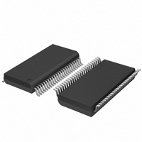
IC UART W/FIFO 48-TSSOP
Manufacturer
NXP Semiconductors
Series
IMPACTr
Datasheet
1.SC28L201A1DGG118.pdf
(110 pages)
Specifications of SC28L201A1DGG,118
Features
False-start Bit Detection
Number Of Channels
2, DUART
Fifo's
256 Byte
Voltage - Supply
3.3V, 5V
With Parallel Port
Yes
With Auto Flow Control
Yes
With False Start Bit Detection
Yes
With Modem Control
Yes
With Cmos
Yes
Mounting Type
Surface Mount
Package / Case
48-TSSOP
Lead Free Status / RoHS Status
Lead free / RoHS Compliant
Other names
935277824118
SC28L201A1DGG-T
SC28L201A1DGG-T
SC28L201A1DGG-T
SC28L201A1DGG-T


Philips Semiconductors
8.2.8
8.2.9
8.2.10
8.2.11
8.2.12
8.2.13
8.2.14
8.2.15
8.3
8.3.1
8.3.2
8.3.3
8.3.4
8.3.5
8.4
8.4.1
8.4.2
8.4.3
8.4.4
8.4.5
8.4.6
8.4.7
8.4.8
8.5
8.5.1
8.5.2
8.5.3
8.5.4
8.5.5
8.5.6
8.5.7
8.5.8
8.5.9
8.5.10
8.5.11
8.5.12
Interrupt Status Register (ISR) . . . . . . . . . . . . 56
Interrupt Mask Register (IMR) . . . . . . . . . . . . 58
Receiver FIFO (RxFIFO) . . . . . . . . . . . . . . . . 59
Transmitter FIFO (TxFIFO) . . . . . . . . . . . . . . . 59
Receiver FIFO Interrupt Level (RxFIL) . . . . . . 59
Receiver FIFO Fill Level register (RxFL) . . . . 60
Transmitter FIFO Interrupt Level (TxFIL) . . . . 60
Transmitter FIFO Empty Level register (TxEL) 60
Registers for character recognition . . . . . . . . . 61
Xon Character Register (XonCR) . . . . . . . . . . 61
Xoff Character Register (XoffCR) . . . . . . . . . . 61
Address Recognition Character Register
(ARCR) . . . . . . . . . . . . . . . . . . . . . . . . . . . . . . 61
Xon/Xoff Interrupt Status Register (XISR) . . . 62
Watchdog, Character, Address and X Enable
Register (WCXER) . . . . . . . . . . . . . . . . . . . . . 63
Programmable counters, timers, and baud rate
generators. . . . . . . . . . . . . . . . . . . . . . . . . . . . 64
Programmable BRG Timer Reload Registers,
Upper 0 and Upper 1 (PBRGPU) . . . . . . . . . . 64
Programmable BRG Timer Reload Registers,
Lower 0 and Lower 1 (PBRGPL) . . . . . . . . . . 64
Counter/Timer clock source (CTCS0 and
CTCS1). . . . . . . . . . . . . . . . . . . . . . . . . . . . . . 65
Counter Timer Value Registers, Upper 0 and
Upper 1 (CTVU0, CTVU1) . . . . . . . . . . . . . . . 66
Counter Timer Value Registers, Lower 0 and
Lower 1 (CTVL0, CTVL1) . . . . . . . . . . . . . . . . 66
Programmable BRG Clock Source, 0 and 1
(PBRGCS) . . . . . . . . . . . . . . . . . . . . . . . . . . . 66
Counter/Timer Preset Upper and Counter/Timer
Preset Lower (CTPU, CTPL) . . . . . . . . . . . . . 67
The CTS, RTS, CTS Enable Tx signals . . . . . 68
Registers of the Arbitrating Interrupt system
and bidding control . . . . . . . . . . . . . . . . . . . . . 69
Interrupt Control Register (ICR) . . . . . . . . . . . 69
Update CIR (UCIR): the most important
command for polled or interrupt service . . . . . 69
Current Interrupt Register (CIR) . . . . . . . . . . . 70
Interrupt Vector Register (IVR) . . . . . . . . . . . . 71
Global Interrupting Channel Register (GICR) . 71
Global Interrupting Byte Count Register
(GIBCR) . . . . . . . . . . . . . . . . . . . . . . . . . . . . . 71
Global Interrupting Type Register (GITR) . . . . 72
Global RxFIFO register (GRxFIFO) . . . . . . . . 72
Global TxFIFO register (GTxFIFO). . . . . . . . . 72
Bidding Control Register, Break Change
(BCRBRK) . . . . . . . . . . . . . . . . . . . . . . . . . . . 73
Bidding Control Register, Change-Of-State
(BCRCOS) . . . . . . . . . . . . . . . . . . . . . . . . . . . 73
Bidding Control Register, Xon/Xoff (BCRx) . . 73
8.5.13
8.5.14
8.5.15
8.6
8.6.1
8.6.2
8.6.3
8.6.4
8.6.5
8.6.6
8.6.7
8.6.8
8.6.9
8.6.10
8.6.11
8.6.12
8.7
9
10
11
12
12.1
13
14
15
15.1
15.2
15.3
15.4
15.5
16
17
18
19
20
21
22
© Koninklijke Philips Electronics N.V. 2005
All rights are reserved. Reproduction in whole or in part is prohibited without the prior
written consent of the copyright owner. The information presented in this document does
not form part of any quotation or contract, is believed to be accurate and reliable and may
be changed without notice. No liability will be accepted by the publisher for any
consequence of its use. Publication thereof does not convey nor imply any license under
patent- or other industrial or intellectual property rights.
Published in The Netherlands
3.3 V, 5 V UART, 3.125 Mbit/s, with 256-byte FIFO
Register maps . . . . . . . . . . . . . . . . . . . . . . . . . 86
Limiting values . . . . . . . . . . . . . . . . . . . . . . . . 90
Static characteristics . . . . . . . . . . . . . . . . . . . 91
Dynamic characteristics . . . . . . . . . . . . . . . . . 93
Test information. . . . . . . . . . . . . . . . . . . . . . . 103
Package outline . . . . . . . . . . . . . . . . . . . . . . . 104
Soldering . . . . . . . . . . . . . . . . . . . . . . . . . . . . 105
Abbreviations . . . . . . . . . . . . . . . . . . . . . . . . 107
Revision history . . . . . . . . . . . . . . . . . . . . . . 107
Data sheet status. . . . . . . . . . . . . . . . . . . . . . 108
Definitions . . . . . . . . . . . . . . . . . . . . . . . . . . . 108
Disclaimers . . . . . . . . . . . . . . . . . . . . . . . . . . 108
Trademarks . . . . . . . . . . . . . . . . . . . . . . . . . . 108
Contact information . . . . . . . . . . . . . . . . . . . 108
Bidding Control Register, Address (BCRA) . . 73
Bidding Control Register, C/T 0 and C/T 1
(BCR C/T) . . . . . . . . . . . . . . . . . . . . . . . . . . . 73
Bidding Control Register, Received Loopback
Error (BCRLBE) . . . . . . . . . . . . . . . . . . . . . . . 73
Registers of the I/O ports . . . . . . . . . . . . . . . . 74
Input Port Change Register Lower Nibble, A
(IPCRL) . . . . . . . . . . . . . . . . . . . . . . . . . . . . . 74
Input Port Change Register Lower Nibble, B
(IPCRL) . . . . . . . . . . . . . . . . . . . . . . . . . . . . . 75
Input Port Change Register Upper Nibble, A
(IPCRU) . . . . . . . . . . . . . . . . . . . . . . . . . . . . . 76
Input Port Change Register Upper Nibble, B
(IPCRU) . . . . . . . . . . . . . . . . . . . . . . . . . . . . . 77
Input Port Register, A (IPR) . . . . . . . . . . . . . . 77
Input Port Register, B (UPT) . . . . . . . . . . . . . 77
Input Change Detect Enable, A (IPCE) . . . . . 78
Input Change Detect Enable, B (IPCE) . . . . . 79
I/O Port Configuration Registers (I/OPCR0,
I/OPCR1, I/OPCR2, I/OPCR3). . . . . . . . . . . . 79
Set the Output Port Bits OPR A and OPR B
(SOPR A and SOPR B) . . . . . . . . . . . . . . . . . 82
Reset Output Port bits OPR A and OPR B
(ROPR A, ROPR B) . . . . . . . . . . . . . . . . . . . . 83
Output Port Register A and B (OPR) . . . . . . 84
BRG characteristics . . . . . . . . . . . . . . . . . . . . 85
Timing diagrams. . . . . . . . . . . . . . . . . . . . . . . 96
Introduction to soldering surface mount
packages . . . . . . . . . . . . . . . . . . . . . . . . . . . 105
Reflow soldering. . . . . . . . . . . . . . . . . . . . . . 105
Wave soldering. . . . . . . . . . . . . . . . . . . . . . . 105
Manual soldering . . . . . . . . . . . . . . . . . . . . . 106
Package related soldering information . . . . . 106
Document number: 9397 750 13138
SC28L201
Date of release: 31 October 2005
Related parts for SC28L201A1DGG,118
Image
Part Number
Description
Manufacturer
Datasheet
Request
R

Part Number:
Description:
NXP Semiconductors designed the LPC2420/2460 microcontroller around a 16-bit/32-bitARM7TDMI-S CPU core with real-time debug interfaces that include both JTAG andembedded trace
Manufacturer:
NXP Semiconductors
Datasheet:

Part Number:
Description:
NXP Semiconductors designed the LPC2458 microcontroller around a 16-bit/32-bitARM7TDMI-S CPU core with real-time debug interfaces that include both JTAG andembedded trace
Manufacturer:
NXP Semiconductors
Datasheet:
Part Number:
Description:
NXP Semiconductors designed the LPC2468 microcontroller around a 16-bit/32-bitARM7TDMI-S CPU core with real-time debug interfaces that include both JTAG andembedded trace
Manufacturer:
NXP Semiconductors
Datasheet:
Part Number:
Description:
NXP Semiconductors designed the LPC2470 microcontroller, powered by theARM7TDMI-S core, to be a highly integrated microcontroller for a wide range ofapplications that require advanced communications and high quality graphic displays
Manufacturer:
NXP Semiconductors
Datasheet:
Part Number:
Description:
NXP Semiconductors designed the LPC2478 microcontroller, powered by theARM7TDMI-S core, to be a highly integrated microcontroller for a wide range ofapplications that require advanced communications and high quality graphic displays
Manufacturer:
NXP Semiconductors
Datasheet:
Part Number:
Description:
The Philips Semiconductors XA (eXtended Architecture) family of 16-bit single-chip microcontrollers is powerful enough to easily handle the requirements of high performance embedded applications, yet inexpensive enough to compete in the market for hi
Manufacturer:
NXP Semiconductors
Datasheet:
Part Number:
Description:
The XA-S3 device is a member of Philips Semiconductors? XA(eXtended Architecture) family of high performance 16-bitsingle-chip microcontrollers
Manufacturer:
NXP Semiconductors
Datasheet:

Part Number:
Description:
The NXP BlueStreak LH75401/LH75411 family consists of two low-cost 16/32-bit System-on-Chip (SoC) devices
Manufacturer:
NXP Semiconductors
Datasheet:
Part Number:
Description:
The NXP LPC3130/3131 combine an 180 MHz ARM926EJ-S CPU core, high-speed USB2
Manufacturer:
NXP Semiconductors
Datasheet:
Part Number:
Description:
The NXP LPC3141 combine a 270 MHz ARM926EJ-S CPU core, High-speed USB 2
Manufacturer:
NXP Semiconductors
Part Number:
Description:
The NXP LPC3143 combine a 270 MHz ARM926EJ-S CPU core, High-speed USB 2
Manufacturer:
NXP Semiconductors

Part Number:
Description:
The NXP LPC3152 combines an 180 MHz ARM926EJ-S CPU core, High-speed USB 2
Manufacturer:
NXP Semiconductors
Part Number:
Description:
The NXP LPC3154 combines an 180 MHz ARM926EJ-S CPU core, High-speed USB 2
Manufacturer:
NXP Semiconductors

Part Number:
Description:
Standard level N-channel enhancement mode Field-Effect Transistor (FET) in a plastic package using NXP High-Performance Automotive (HPA) TrenchMOS technology
Manufacturer:
NXP Semiconductors
Datasheet: