SC28L201A1DGG,118 NXP Semiconductors, SC28L201A1DGG,118 Datasheet - Page 49
SC28L201A1DGG,118
Manufacturer Part Number
SC28L201A1DGG,118
Description
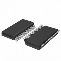
IC UART W/FIFO 48-TSSOP
Manufacturer
NXP Semiconductors
Series
IMPACTr
Datasheet
1.SC28L201A1DGG118.pdf
(110 pages)
Specifications of SC28L201A1DGG,118
Features
False-start Bit Detection
Number Of Channels
2, DUART
Fifo's
256 Byte
Voltage - Supply
3.3V, 5V
With Parallel Port
Yes
With Auto Flow Control
Yes
With False Start Bit Detection
Yes
With Modem Control
Yes
With Cmos
Yes
Mounting Type
Surface Mount
Package / Case
48-TSSOP
Lead Free Status / RoHS Status
Lead free / RoHS Compliant
Other names
935277824118
SC28L201A1DGG-T
SC28L201A1DGG-T
SC28L201A1DGG-T
SC28L201A1DGG-T


Philips Semiconductors
9397 750 13138
Product data sheet
8.2.5 Receiver Clock Select Register (RxCSR) and Transmitter Clock Select
Table 19:
[1]
Register (TxCSR)
Table 20:
Both registers consist of single 6-bit field that selects the clock source for the receiver and
transmitter respectively. During a read the unused bits in this register read ‘000’. The
‘BRG’ baud rates (fixed BRG rates) shown in
frequency of 14.7456 MHz. The baud rates shown in
crystal clock varies. For example, if the SCLK rate is changed to 7.3728 MHz all the rates
below will reduce by
Bit
1:0
Bit
7:6
5:0
If this bit is not ‘0’, the characters will be stripped regardless of bits [3:2] or [1:0].
Symbol
Symbol
-
-
MR3 - Mode Register 3 (address 0x23) bit description
RxCSR - Receiver Clock Select Register (address 0x30) and
TxCSR - Transmitter Clock Select Register (address 0x31) bit description
Description
Address Recognition control.
This field controls the operation of the Address recognition logic. If the device
is not operating in the special or Wake-up mode, this hardware may be used
as a general-purpose character detector by choosing any combination except
00. Interrupt generation is controlled by the channel IMR. The interrupt may be
cleared by a read of the XISR, the Xon/Xoff Interrupt Status Register. See
further description in
Description
reserved
Transmitter/Receiver Clock Select code; see
00 = default
01 = Auto wake
10 = Auto doze
11 = Auto wake and Auto doze
1
Rev. 01 — 31 October 2005
2
.
Section 7.4.7.6 “Wake-up
3.3 V, 5 V UART, 3.125 Mbit/s, with 256-byte FIFO
Table 21
Table 21
are based on the SCLK crystal
© Koninklijke Philips Electronics N.V. 2005. All rights reserved.
Table
mode”.
will vary as the SCLK
…continued
21.
SC28L201
49 of 110
Related parts for SC28L201A1DGG,118
Image
Part Number
Description
Manufacturer
Datasheet
Request
R

Part Number:
Description:
NXP Semiconductors designed the LPC2420/2460 microcontroller around a 16-bit/32-bitARM7TDMI-S CPU core with real-time debug interfaces that include both JTAG andembedded trace
Manufacturer:
NXP Semiconductors
Datasheet:

Part Number:
Description:
NXP Semiconductors designed the LPC2458 microcontroller around a 16-bit/32-bitARM7TDMI-S CPU core with real-time debug interfaces that include both JTAG andembedded trace
Manufacturer:
NXP Semiconductors
Datasheet:
Part Number:
Description:
NXP Semiconductors designed the LPC2468 microcontroller around a 16-bit/32-bitARM7TDMI-S CPU core with real-time debug interfaces that include both JTAG andembedded trace
Manufacturer:
NXP Semiconductors
Datasheet:
Part Number:
Description:
NXP Semiconductors designed the LPC2470 microcontroller, powered by theARM7TDMI-S core, to be a highly integrated microcontroller for a wide range ofapplications that require advanced communications and high quality graphic displays
Manufacturer:
NXP Semiconductors
Datasheet:
Part Number:
Description:
NXP Semiconductors designed the LPC2478 microcontroller, powered by theARM7TDMI-S core, to be a highly integrated microcontroller for a wide range ofapplications that require advanced communications and high quality graphic displays
Manufacturer:
NXP Semiconductors
Datasheet:
Part Number:
Description:
The Philips Semiconductors XA (eXtended Architecture) family of 16-bit single-chip microcontrollers is powerful enough to easily handle the requirements of high performance embedded applications, yet inexpensive enough to compete in the market for hi
Manufacturer:
NXP Semiconductors
Datasheet:
Part Number:
Description:
The XA-S3 device is a member of Philips Semiconductors? XA(eXtended Architecture) family of high performance 16-bitsingle-chip microcontrollers
Manufacturer:
NXP Semiconductors
Datasheet:

Part Number:
Description:
The NXP BlueStreak LH75401/LH75411 family consists of two low-cost 16/32-bit System-on-Chip (SoC) devices
Manufacturer:
NXP Semiconductors
Datasheet:
Part Number:
Description:
The NXP LPC3130/3131 combine an 180 MHz ARM926EJ-S CPU core, high-speed USB2
Manufacturer:
NXP Semiconductors
Datasheet:
Part Number:
Description:
The NXP LPC3141 combine a 270 MHz ARM926EJ-S CPU core, High-speed USB 2
Manufacturer:
NXP Semiconductors
Part Number:
Description:
The NXP LPC3143 combine a 270 MHz ARM926EJ-S CPU core, High-speed USB 2
Manufacturer:
NXP Semiconductors

Part Number:
Description:
The NXP LPC3152 combines an 180 MHz ARM926EJ-S CPU core, High-speed USB 2
Manufacturer:
NXP Semiconductors
Part Number:
Description:
The NXP LPC3154 combines an 180 MHz ARM926EJ-S CPU core, High-speed USB 2
Manufacturer:
NXP Semiconductors

Part Number:
Description:
Standard level N-channel enhancement mode Field-Effect Transistor (FET) in a plastic package using NXP High-Performance Automotive (HPA) TrenchMOS technology
Manufacturer:
NXP Semiconductors
Datasheet: