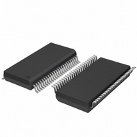
SC28L201A1DGG,118 NXP Semiconductors, SC28L201A1DGG,118 Datasheet - Page 44

SC28L201A1DGG,118
Manufacturer Part Number
SC28L201A1DGG,118
Description
IC UART W/FIFO 48-TSSOP
Manufacturer
NXP Semiconductors
Series
IMPACTr
Datasheet
1.SC28L201A1DGG118.pdf
(110 pages)
Specifications of SC28L201A1DGG,118
Features
False-start Bit Detection
Number Of Channels
2, DUART
Fifo's
256 Byte
Voltage - Supply
3.3V, 5V
With Parallel Port
Yes
With Auto Flow Control
Yes
With False Start Bit Detection
Yes
With Modem Control
Yes
With Cmos
Yes
Mounting Type
Surface Mount
Package / Case
48-TSSOP
Lead Free Status / RoHS Status
Lead free / RoHS Compliant
Other names
935277824118
SC28L201A1DGG-T
SC28L201A1DGG-T
SC28L201A1DGG-T
SC28L201A1DGG-T
Philips Semiconductors
9397 750 13138
Product data sheet
8.2.2 Mode Register 1 (MR1)
MR1 can be accessed directly at 0x21 in the Extended section of the address map, or by
means of the MR Pointers at 0x00 used by legacy code.
Table 17:
Bit
7
6
5
Symbol
MR1 - Mode Register 1 (address 0x21) bit description
Description
RxRTS control. Receiver Request-to-Send (hardware flow control)
This bit controls the deactivation of the RTSN output (I/O2) by the receiver.
The I/O2 output is asserted and negated by commands applied via the
command register or through the setting of the OPR register bits. MR1[7] = 1
enables the receiver state machine to control the state of the I/O2 (where the
RTSN function is assigned) to be automatically negated (driven HIGH) upon
receipt of a valid start bit if the receiver FIFO is 240 full or greater (for 8-byte
mode the FIFO full signal is used). RTSN is reasserted when the FIFO fill
level falls below 240 filled FIFO positions. This constitutes a change from
previous members of Philips UART families where the RTSN function
triggered on FIFO full. This behavior caused problems with PC UARTs that
could not stop transmission at the proper time.
Remark: When the FIFO is set to an 8-byte depth, the RTSN signaling is
triggered on position 8 of the FIFO.
The RTSN feature can be used to prevent overrun in the receiver by using
the RTSN output signal to control the CTSN (see description of bit MR2[4] in
Table 18 “MR2 - Mode Register 2 (address 0x22) bit
transmitting device. It is not recommend to use the hardware flow control and
the in-band (Xon/Xoff) flow control at the same time, although the UART
hardware will allow it.
To use the RTSN function:
Receiver interrupt control bit 1. See description under MR0[6]. (Writing to
this register will reset the RxFIFO interrupt to the bit configuration of MR0
and MR1. Reading has no effect.)
Refer to
Error Mode. Error Mode Select and sub-modes.
This bit selects the operating mode of the three FIFOed status bits (FE, PE,
and received break). In the character mode, status is provided on a
character-by-character basis. The status applies only to the character at the
output of the FIFO.
In the block mode, the status provided in the SR for these bits is the
accumulation (logical OR) of the status for all characters coming to the
output of the FIFO, since the last reset error command was issued.
The Block Error mode has two-sub modes. These modes are controlled by
the Command Register. The error is accumulated (as described above) at
either the entry of the data in to the FIFO or on the exit (read of the FIFO). Of
the two the setting of the error on the entry of the data into the FIFO gives the
earliest warning of error data.
1. Set MR1[7] to 1.
2. Set I/O0B as appropriate to logical 0.
3. Enable receiver.
0 = off
1 = on
0 = character
1 = block (entry or exit)
Rev. 01 — 31 October 2005
Table 13
and
3.3 V, 5 V UART, 3.125 Mbit/s, with 256-byte FIFO
Table 14
in
Section 8.2.1 “Mode Register 0
© Koninklijke Philips Electronics N.V. 2005. All rights reserved.
description”) input of the
SC28L201
(MR0)”.
44 of 110


