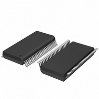
SC28L201A1DGG,118 NXP Semiconductors, SC28L201A1DGG,118 Datasheet - Page 59

SC28L201A1DGG,118
Manufacturer Part Number
SC28L201A1DGG,118
Description
IC UART W/FIFO 48-TSSOP
Manufacturer
NXP Semiconductors
Series
IMPACTr
Datasheet
1.SC28L201A1DGG118.pdf
(110 pages)
Specifications of SC28L201A1DGG,118
Features
False-start Bit Detection
Number Of Channels
2, DUART
Fifo's
256 Byte
Voltage - Supply
3.3V, 5V
With Parallel Port
Yes
With Auto Flow Control
Yes
With False Start Bit Detection
Yes
With Modem Control
Yes
With Cmos
Yes
Mounting Type
Surface Mount
Package / Case
48-TSSOP
Lead Free Status / RoHS Status
Lead free / RoHS Compliant
Other names
935277824118
SC28L201A1DGG-T
SC28L201A1DGG-T
SC28L201A1DGG-T
SC28L201A1DGG-T
Philips Semiconductors
9397 750 13138
Product data sheet
8.2.10 Receiver FIFO (RxFIFO)
8.2.11 Transmitter FIFO (TxFIFO)
8.2.12 Receiver FIFO Interrupt Level (RxFIL)
The FIFO for the receiver is 11 bits wide and 256 words deep. The status of each byte
received is stored with that byte and is moved along with the byte as the characters are
read from the FIFO. The upper three bits are presented in the Status Register and they
change in the Status Register each time a data byte is read from the FIFO. Therefore, the
Status Register should be read before the byte is read from the RxFIFO if one wishes to
ascertain the quality of the byte.
The foregoing applies to the ‘character error mode’ of status reporting. See MR1[5] in
Table 17
gives the accumulated error of all bytes received by the RxFIFO since the last Reset Error
command was issued (CR = 0x04).
Table 27:
[1]
The FIFO for the transmitter is 8 bits wide by 256 bytes deep. For character lengths less
than 8 bits, the upper bits will be ignored by the transmitter state machine and thus are
effectively discarded.
Table 28:
The position in the RxFIFO that causes the receiver will enter the interrupt arbitration
process. This register is used to offset the effect of the arbitration threshold. It use may
yield moderate improvements in the interrupt service. It will also ‘equalize’ interrupt
latency and allow for larger aggregate block transfers between fast and slow channels.
Writing to this register removes the interrupt control established in MR0 and MR1.
Table 29:
Bit
10
9
8
7:0
Bit
7:0
Bit
7:0
[1]
[1]
[1]
These bits are sent to the Status Register.
Symbol
Symbol
Symbol
and RxFIFO descriptions for ‘block error’ status reporting. Briefly, Block Error
RxFIFO - Receiver FIFO register (address 0x03) bit description
TxFIFO - Transmitter FIFO register (address 0x03) bit description
RxFIL - Receiver FIFO Interrupt Level register (address 0x46) bit description
Description
break received status
framing error status
parity error status
This is the data byte sent to the data bus on RxFIFO read.
8 data bits. MSBs = 0 for 7, 6, 5 bit data.
Description
8 data bits. MSBs are ignored to 0 for 7, 6, 5 bit data.
Description
any one of 256 FIFO fill positions
Rev. 01 — 31 October 2005
3.3 V, 5 V UART, 3.125 Mbit/s, with 256-byte FIFO
© Koninklijke Philips Electronics N.V. 2005. All rights reserved.
SC28L201
59 of 110


