SC28L201A1DGG,118 NXP Semiconductors, SC28L201A1DGG,118 Datasheet - Page 17
SC28L201A1DGG,118
Manufacturer Part Number
SC28L201A1DGG,118
Description
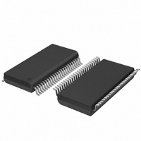
IC UART W/FIFO 48-TSSOP
Manufacturer
NXP Semiconductors
Series
IMPACTr
Datasheet
1.SC28L201A1DGG118.pdf
(110 pages)
Specifications of SC28L201A1DGG,118
Features
False-start Bit Detection
Number Of Channels
2, DUART
Fifo's
256 Byte
Voltage - Supply
3.3V, 5V
With Parallel Port
Yes
With Auto Flow Control
Yes
With False Start Bit Detection
Yes
With Modem Control
Yes
With Cmos
Yes
Mounting Type
Surface Mount
Package / Case
48-TSSOP
Lead Free Status / RoHS Status
Lead free / RoHS Compliant
Other names
935277824118
SC28L201A1DGG-T
SC28L201A1DGG-T
SC28L201A1DGG-T
SC28L201A1DGG-T


Philips Semiconductors
9397 750 13138
Product data sheet
7.3.1 Input characteristics of the I/O ports
7.3.2 Output port of the I/O ports
7.3 I/O ports
Each timer unit has eight different clock sources available to it, as described in
8.4.6 “Programmable BRG Clock Source, 0 and 1
stop controls are also contained in this register. The PBRG counters generate a
symmetrical square wave whose half period is equal in time to the division of the selected
PBRG Timer clock source by the number loaded to the PBRGPU and PBRGPL Preset
Registers. Thus, the output frequency will be the clock source frequency divided by twice
the 16-bit value loaded to these registers. This is the result of counting down once for the
high portion of the output wave and once for the low portion.
Whenever the these timers are selected via the receiver or transmitter Clock Select
register, their output will be configured as a 16 clock for the respective receiver or
transmitter. Therefore, one needs to program the timers to generate a clock 16 times
faster than the data rate. The formula for calculating ‘n’, the number loaded to the
PBRGPL and PBRGPU registers, is the same as shown in
Thirteen (13) I/O ports are provided for the UART. They may be programmed to be inputs
or outputs. The input circuits are always active whether programmed as and input or an
output. In general a 2-bit code in the I/OPCR (I/O Port Control Register) controls what
function these pins will present. All I/O ports default to high-impedance input state on
power-up. All 13 I/O pins have a small pull-up ‘resistor’ that provides approximately 5 A
current.
Remark: When calling software written for legacy two-channel UARTs manufactured by
Philips (Signetics), be sure I/O pins are set to input where the legacy software expected
an input. Declare I/O pins as output where the legacy software expected an output.
The I/O pins are configured individually to be inputs or outputs. As inputs they may be
used to bring external data to the bus, as clocks for internal functions or external control
signals. Each I/O pin has a ‘Change-of-State’ detector. The change detectors are used to
signal a change in the signal level at the pin (either 0-to-1 or 1-to-0 transitions). The level
change on these pins must be stable for approximately 25 s to 50 s (two edges of the
internally generated 38.4 kHz baud rate clock) before the detectors will signal a valid
change. These are typically used for interface signals from modems to the UART and from
there to the host.
The OPR, I/OPCR, MR, and CR registers may control the I/O pins when configured as
outputs. (For the control in the lower 16 position address space, the control register is the
OPCR.) Via appropriate programming, the pins of the output port may be configured as
another parallel port to external circuits, or they may represent internal conditions of the
UART. When this 8-bit port is used as a general-purpose output port, the output port pins
drive inverse logic levels of the individual bits in the Output Port Register (OPR). The OPR
register is set and reset by writing to the SOPR and ROPR addresses
“Bidding Control Register, Break Change (BCRBRK)”
Register, Change-Of-State
of the OPR registers. The I/OPCR (or the OPCR) register conditions these output pins to
be controlled by the OPR or by other signals in the chip. Output ports are driven HIGH on
hardware reset.
Rev. 01 — 31 October 2005
(BCRCOS)”). The output pins will drive the same data polarity
3.3 V, 5 V UART, 3.125 Mbit/s, with 256-byte FIFO
(PBRGCS)”. Note that the timer run and
and
Section 8.5.11 “Bidding Control
© Koninklijke Philips Electronics N.V. 2005. All rights reserved.
Equation
SC28L201
1.
(seeSection 8.5.10
Section
17 of 110
Related parts for SC28L201A1DGG,118
Image
Part Number
Description
Manufacturer
Datasheet
Request
R

Part Number:
Description:
NXP Semiconductors designed the LPC2420/2460 microcontroller around a 16-bit/32-bitARM7TDMI-S CPU core with real-time debug interfaces that include both JTAG andembedded trace
Manufacturer:
NXP Semiconductors
Datasheet:

Part Number:
Description:
NXP Semiconductors designed the LPC2458 microcontroller around a 16-bit/32-bitARM7TDMI-S CPU core with real-time debug interfaces that include both JTAG andembedded trace
Manufacturer:
NXP Semiconductors
Datasheet:
Part Number:
Description:
NXP Semiconductors designed the LPC2468 microcontroller around a 16-bit/32-bitARM7TDMI-S CPU core with real-time debug interfaces that include both JTAG andembedded trace
Manufacturer:
NXP Semiconductors
Datasheet:
Part Number:
Description:
NXP Semiconductors designed the LPC2470 microcontroller, powered by theARM7TDMI-S core, to be a highly integrated microcontroller for a wide range ofapplications that require advanced communications and high quality graphic displays
Manufacturer:
NXP Semiconductors
Datasheet:
Part Number:
Description:
NXP Semiconductors designed the LPC2478 microcontroller, powered by theARM7TDMI-S core, to be a highly integrated microcontroller for a wide range ofapplications that require advanced communications and high quality graphic displays
Manufacturer:
NXP Semiconductors
Datasheet:
Part Number:
Description:
The Philips Semiconductors XA (eXtended Architecture) family of 16-bit single-chip microcontrollers is powerful enough to easily handle the requirements of high performance embedded applications, yet inexpensive enough to compete in the market for hi
Manufacturer:
NXP Semiconductors
Datasheet:
Part Number:
Description:
The XA-S3 device is a member of Philips Semiconductors? XA(eXtended Architecture) family of high performance 16-bitsingle-chip microcontrollers
Manufacturer:
NXP Semiconductors
Datasheet:

Part Number:
Description:
The NXP BlueStreak LH75401/LH75411 family consists of two low-cost 16/32-bit System-on-Chip (SoC) devices
Manufacturer:
NXP Semiconductors
Datasheet:
Part Number:
Description:
The NXP LPC3130/3131 combine an 180 MHz ARM926EJ-S CPU core, high-speed USB2
Manufacturer:
NXP Semiconductors
Datasheet:
Part Number:
Description:
The NXP LPC3141 combine a 270 MHz ARM926EJ-S CPU core, High-speed USB 2
Manufacturer:
NXP Semiconductors
Part Number:
Description:
The NXP LPC3143 combine a 270 MHz ARM926EJ-S CPU core, High-speed USB 2
Manufacturer:
NXP Semiconductors

Part Number:
Description:
The NXP LPC3152 combines an 180 MHz ARM926EJ-S CPU core, High-speed USB 2
Manufacturer:
NXP Semiconductors
Part Number:
Description:
The NXP LPC3154 combines an 180 MHz ARM926EJ-S CPU core, High-speed USB 2
Manufacturer:
NXP Semiconductors

Part Number:
Description:
Standard level N-channel enhancement mode Field-Effect Transistor (FET) in a plastic package using NXP High-Performance Automotive (HPA) TrenchMOS technology
Manufacturer:
NXP Semiconductors
Datasheet: