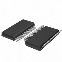
SC28L201A1DGG,118 NXP Semiconductors, SC28L201A1DGG,118 Datasheet - Page 16

SC28L201A1DGG,118
Manufacturer Part Number
SC28L201A1DGG,118
Description
IC UART W/FIFO 48-TSSOP
Manufacturer
NXP Semiconductors
Series
IMPACTr
Datasheet
1.SC28L201A1DGG118.pdf
(110 pages)
Specifications of SC28L201A1DGG,118
Features
False-start Bit Detection
Number Of Channels
2, DUART
Fifo's
256 Byte
Voltage - Supply
3.3V, 5V
With Parallel Port
Yes
With Auto Flow Control
Yes
With False Start Bit Detection
Yes
With Modem Control
Yes
With Cmos
Yes
Mounting Type
Surface Mount
Package / Case
48-TSSOP
Lead Free Status / RoHS Status
Lead free / RoHS Compliant
Other names
935277824118
SC28L201A1DGG-T
SC28L201A1DGG-T
SC28L201A1DGG-T
SC28L201A1DGG-T
Philips Semiconductors
9397 750 13138
Product data sheet
7.2.4 Programmable Baud Rate Generators (PBRG)
RXFIFO that has not been read. The Counter/Timer uses the numbers loaded into the
Counter/Timer Lower Register (CTPL and the Counter/Timer Upper Register (CTPU) as
its divisor. The counter/timer is controlled with six commands: Start/Stop C/T, Read/Write
Counter/Timer lower register and Read/Write Counter/Timer upper register. These
commands have slight differences depending on the mode of operation. Please see the
detail of the commands under
Counter/Timer Preset Lower (CTPU,
Whenever the these timers are selected via the receiver or transmitter Clock Select
register, their output will be configured as a 16 clock for the respective receiver or
transmitter. Therefore, one needs to program the timers to generate a clock 16 times
faster than the data rate. The formula for calculating ‘n’, the number loaded to the CTPU
and CTPL registers, based on a particular input clock frequency is shown in
For the Timer mode, the formula is as follows:
(If the pulse mode is selected, then ‘2’ in the divisor should be ‘1’. This doubles the C/T
output speeds for any given input clock.)
Remark: ‘n’ may assume a value of 1. In previous Philips data communications
controllers this value was not allowed. The Counter/Timer Clock Select Register (CTCS)
controls the Counter/Timer input frequency.
The frequency generated from the above formula will be at a rate 16 times faster than the
desired baud rate. The transmitter and receiver state machines include divide-by-16
circuits, which provide the final frequency and provide various timing edges used in the
qualifying the serial data bit stream.
Often this division will result in a non-integer value: 26.3 for example. One may only
program integer numbers to a digital divider. Therefore, 26 (0x001A) would be chosen. If
26.7 were the result of the division then 27 (0x001B) would be chosen. This gives a baud
rate error of 0.3/26.3 or 0.3/26.7 that yields a percentage error of 1.14 % or 1.12 %
respectively, well within the ability of the asynchronous mode of operation. Higher input
frequency to the counter reduces the error effect of the fractional division.
One should be cautious about the assumed benign effects of small errors since the other
receiver or transmitter with which one is communicating may also have a small error in the
precise baud rate. In a clean communications environment using one START bit, eight
data bits, and one STOP bit, the total difference allowed between the transmitter and
receiver frequency is approximately 4.6 %. Less than eight data bits will increase this
percentage.
There are two PBRG Counters, used only for random baud rate generation. The two
PBRG Timers are programmable 16-bit dividers that are used for generating
miscellaneous clocks. These clocks may be used by the receiver, transmitter,
counter/timers or I/O pin at any time in any combination.
n
=
------------------------------------------------------------------ -
C/T clock input frequency
2 16 desired baud rate
Rev. 01 — 31 October 2005
Section 8.4.7 “Counter/Timer Preset Upper and
CTPL)”.
3.3 V, 5 V UART, 3.125 Mbit/s, with 256-byte FIFO
© Koninklijke Philips Electronics N.V. 2005. All rights reserved.
SC28L201
Equation
16 of 110
1.
(1)


