DK-DEV-2AGX125N Altera, DK-DEV-2AGX125N Datasheet - Page 8
DK-DEV-2AGX125N
Manufacturer Part Number
DK-DEV-2AGX125N
Description
KIT DEV ARRIA II GX FPGA 2AGX125
Manufacturer
Altera
Series
Arria II GXr
Type
FPGAr
Datasheets
1.EP2AGX45CU17C6N.pdf
(96 pages)
2.DK-DEV-2AGX125N.pdf
(48 pages)
3.DK-DEV-2AGX125N.pdf
(64 pages)
Specifications of DK-DEV-2AGX125N
Contents
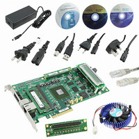
Board, Cables, CD, DVD, Power Supply
Silicon Manufacturer
Altera
Core Architecture
FPGA
Core Sub-architecture
Arria
Silicon Core Number
EP2
Silicon Family Name
Arria II GX
Rohs Compliant
Yes
For Use With/related Products
EP2AGX125EF35
Lead Free Status / RoHS Status
Lead free / RoHS Compliant
Other names
544-2600
Available stocks
Company
Part Number
Manufacturer
Quantity
Price
Company:

Part Number:
DK-DEV-2AGX125N
Manufacturer:
Altera
Quantity:
135


1–4
Development Board Block Diagram
Figure 1–1. Arria II GX FPGA Development Board Block Diagram
Handling the Board
Arria II GX FPGA Development Board Reference Manual
100 M, 125 M, 156.25 M,
Programmable Oscillator
100 M, 125 M, 156.25 M,
Programmable Oscillator
DDR2 SODIMM (x64)
Gigabit Ethernet
Clock SMA OUT
SMA (LVPECL)
PHY (RGMII)
1 Gbyte
*Port B is only connected on
EP2AGX260EF35 devices.
c
c
155.52 MHz
Figure 1–1
When handling the board, it is important to observe the following precaution:
Without proper anti-static handling, the board can be damaged. Therefore, use
anti-static handling precautions when touching the board.
In order to avoid damaging the board due to voltage spikes, place the power switch
(SW1) in the OFF position prior to plugging in the DC Input power jack.
x1 REF CLK
x3 REF CLK
x1 CLK IN
x1 CLK IN
x1 REF CLK
x120
x16
x1
shows the block diagram of the Arria II GX FPGA development board.
Port B*
x8 Edge
EP2AGX125EF35
CPLD
Port A
64 Mbyte
Flash
x50
x11
x26 ADDR
x32 DATA
February 2011 Altera Corporation
x4
x4
Development Board Block Diagram
x3
USB
2.0
JTAG Chain
Push-button
DDR3 (x16)
128 Mbyte
DIP Switch
2x16 LCD
Chapter 1: Overview
2 Mbyte
Switches
SSRAM
LEDs
Embedded
Blaster
Z Z
Related parts for DK-DEV-2AGX125N
Image
Part Number
Description
Manufacturer
Datasheet
Request
R

Part Number:
Description:
KIT DEV CYCLONE III LS EP3CLS200
Manufacturer:
Altera
Datasheet:

Part Number:
Description:
KIT DEV STRATIX IV FPGA 4SE530
Manufacturer:
Altera
Datasheet:

Part Number:
Description:
KIT DEV FPGA 2AGX260 W/6.375G TX
Manufacturer:
Altera
Datasheet:

Part Number:
Description:
KIT DEV MAX V 5M570Z
Manufacturer:
Altera
Datasheet:

Part Number:
Description:
KIT DEV STRATIX V FPGA 5SGXEA7
Manufacturer:
Altera
Datasheet:

Part Number:
Description:
KIT DEVELOPMENT STRATIX III
Manufacturer:
Altera
Datasheet:

Part Number:
Description:
KIT DEVELOPMENT STRATIX IV
Manufacturer:
Altera
Datasheet:

Part Number:
Description:
KIT DEV ARRIA GX 1AGX60N
Manufacturer:
Altera
Datasheet:
Part Number:
Description:
KIT STARTER CYCLONE IV GX
Manufacturer:
Altera
Datasheet:
Part Number:
Description:
KIT DEVELOPMENT STRATIX IV
Manufacturer:
Altera
Datasheet:

Part Number:
Description:
CPLD, EP610 Family, ECMOS Process, 300 Gates, 16 Macro Cells, 16 Reg., 16 User I/Os, 5V Supply, 35 Speed Grade, 24DIP
Manufacturer:
Altera Corporation
Datasheet:
Part Number:
Description:
CPLD, EP610 Family, ECMOS Process, 300 Gates, 16 Macro Cells, 16 Reg., 16 User I/Os, 5V Supply, 15 Speed Grade, 24DIP
Manufacturer:
Altera Corporation
Datasheet: