DK-DEV-2AGX125N Altera, DK-DEV-2AGX125N Datasheet - Page 14
DK-DEV-2AGX125N
Manufacturer Part Number
DK-DEV-2AGX125N
Description
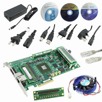
KIT DEV ARRIA II GX FPGA 2AGX125
Manufacturer
Altera
Series
Arria II GXr
Type
FPGAr
Datasheets
1.EP2AGX45CU17C6N.pdf
(96 pages)
2.DK-DEV-2AGX125N.pdf
(48 pages)
3.DK-DEV-2AGX125N.pdf
(64 pages)
Specifications of DK-DEV-2AGX125N
Contents
Board, Cables, CD, DVD, Power Supply
Silicon Manufacturer
Altera
Core Architecture
FPGA
Core Sub-architecture
Arria
Silicon Core Number
EP2
Silicon Family Name
Arria II GX
Rohs Compliant
Yes
For Use With/related Products
EP2AGX125EF35
Lead Free Status / RoHS Status
Lead free / RoHS Compliant
Other names
544-2600
Available stocks
Company
Part Number
Manufacturer
Quantity
Price
Company:

Part Number:
DK-DEV-2AGX125N
Manufacturer:
Altera
Quantity:
135


2–6
Table 2–4. I/O Count for the EP2AGX125 and EP2AGX260 Device
Table 2–5. Arria II GX Device Pin Count and Usage
Table 2–6. Arria II GX Device EP2AGX260EF35 Features
Arria II GX FPGA Development Board Reference Manual
Package
1152-pin Flip Chip
FBGA
Note to
(1) Transceiver signals are not included.
DDR3 ×16 Port
DDR2 SODIMM ×64 Port
MAX Bus
Flash, SRAM, FSM Bus
PCI Express ×8
HSMC Port A
HSMC Port B
Gigabit Ethernet
Buttons
Switches
LCD
LEDs
Clocks or Oscillators
Device I/O Total:
Note to
(1) The HSMC port B is populated when the board uses an EP2AGX260 device. To support the HSMC port B, there are two additional LEDs and a
102,600
ALMs
REFCLK in quadrant 3.
Table
Table
Migration Support
Function
2–4:
2–5:
(1)
Equivalent
256,500
LEs
Device
EP2AGX125 70
EP2AGX260 70
Table 2–4
Table 2–5
development board.
Although the target FPGA for this development board is the EP2AGX125EF35 device,
the first device released in this 40nm FPGA family, the board supports migration to
the largest Arria II GX device, the EP2AGX260EF35.
Table 2–6
M9K RAM
Blocks
2.5-V CMOS + LVDS + LVPECL
950
lists the I/O count for the EP2AGX125 and EP2AGX260 device.
lists the Arria II GX device pin count and usage by function on the
describes the features of the Arria II GX EP2AGX260EF35 device.
2.5-V CMOS + LVDS + XCVR
3A
2.5-V CMOS + XCVR
2.5-V CMOS + XCVR
2.5-V CMOS + LVDS
1.8-V + 2.5-V CMOS
32
—
I/O Standard
3B
1.5-V CMOS
2.5-V CMOS
2.5-V CMOS
2.5-V CMOS
2.5-V CMOS
1.5-V SSTL
1.8-V SSTL
Total RAM
11,756
Kbits
74
74
4A
16
32
4B
18-bit × 18-bit
Multipliers
66
66
5A
736
—
32
5B
458/564
13/15
I/O Count
Bank
7/9
120
104
102
49
82
41
16
11
66
66
8
3
4
6A
(1)
(1)
(1)
PLLs
6
—
32
6B
2 Diff ×8 DQS
8 Diff ×8 DQS
—
—
1 REFCLK, 8 XCVR
4 XCVR, 17 LVDS, 5 Clock Inputs
4 XCVR, 1 Clock Input
1 Clock Input
1 DEV_CLRn
—
—
—
5 REFCLK
70
70
Transceivers
7A
16
16
32
February 2011 Altera Corporation
Featured Device: Arria II GX Device
7B
Special Pins
Chapter 2: Board Components
74
74
8A
1152-pin FBGA
Package Type
—
32
8B
452
612
Total
(1)
Related parts for DK-DEV-2AGX125N
Image
Part Number
Description
Manufacturer
Datasheet
Request
R

Part Number:
Description:
KIT DEV CYCLONE III LS EP3CLS200
Manufacturer:
Altera
Datasheet:

Part Number:
Description:
KIT DEV STRATIX IV FPGA 4SE530
Manufacturer:
Altera
Datasheet:

Part Number:
Description:
KIT DEV FPGA 2AGX260 W/6.375G TX
Manufacturer:
Altera
Datasheet:

Part Number:
Description:
KIT DEV MAX V 5M570Z
Manufacturer:
Altera
Datasheet:

Part Number:
Description:
KIT DEV STRATIX V FPGA 5SGXEA7
Manufacturer:
Altera
Datasheet:

Part Number:
Description:
KIT DEVELOPMENT STRATIX III
Manufacturer:
Altera
Datasheet:

Part Number:
Description:
KIT DEVELOPMENT STRATIX IV
Manufacturer:
Altera
Datasheet:

Part Number:
Description:
KIT DEV ARRIA GX 1AGX60N
Manufacturer:
Altera
Datasheet:
Part Number:
Description:
KIT STARTER CYCLONE IV GX
Manufacturer:
Altera
Datasheet:
Part Number:
Description:
KIT DEVELOPMENT STRATIX IV
Manufacturer:
Altera
Datasheet:

Part Number:
Description:
CPLD, EP610 Family, ECMOS Process, 300 Gates, 16 Macro Cells, 16 Reg., 16 User I/Os, 5V Supply, 35 Speed Grade, 24DIP
Manufacturer:
Altera Corporation
Datasheet:
Part Number:
Description:
CPLD, EP610 Family, ECMOS Process, 300 Gates, 16 Macro Cells, 16 Reg., 16 User I/Os, 5V Supply, 15 Speed Grade, 24DIP
Manufacturer:
Altera Corporation
Datasheet: