DK-DEV-2AGX125N Altera, DK-DEV-2AGX125N Datasheet - Page 30
DK-DEV-2AGX125N
Manufacturer Part Number
DK-DEV-2AGX125N
Description
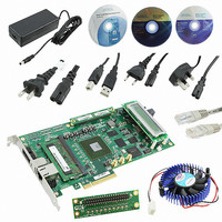
KIT DEV ARRIA II GX FPGA 2AGX125
Manufacturer
Altera
Series
Arria II GXr
Type
FPGAr
Datasheets
1.EP2AGX45CU17C6N.pdf
(96 pages)
2.DK-DEV-2AGX125N.pdf
(48 pages)
3.DK-DEV-2AGX125N.pdf
(64 pages)
Specifications of DK-DEV-2AGX125N
Contents
Board, Cables, CD, DVD, Power Supply
Silicon Manufacturer
Altera
Core Architecture
FPGA
Core Sub-architecture
Arria
Silicon Core Number
EP2
Silicon Family Name
Arria II GX
Rohs Compliant
Yes
For Use With/related Products
EP2AGX125EF35
Lead Free Status / RoHS Status
Lead free / RoHS Compliant
Other names
544-2600
Available stocks
Company
Part Number
Manufacturer
Quantity
Price
Company:

Part Number:
DK-DEV-2AGX125N
Manufacturer:
Altera
Quantity:
135


2–22
Table 2–20. Arria II GX FPGA Development Board Clock Inputs (Part 2 of 2)
Arria II GX FPGA Development Board Reference Manual
SMA or
100.000 MHz
(Default
Frequency)
125.000 MHz
(Default
Frequency)
Samtec HSMC
Samtec HSMC
Samtec HSMC
Samtec HSMC
PCI Express
Edge
Notes to
(1) CDCM61001 has a default frequency of 100 MHz, but can also be set by the MAX II CPLD to frequencies of 125 MHz and 156.25 MHz.
(2) CDCM61004 has a default frequency of 125 MHz, but can also be set by the MAX II CPLD to frequencies of 100 MHz and 156.25 MHz.
(3) Transceiver Q3 is only available when the Arria II GX FPGA development board is populated with the EP2AGX260 device.
(4) HSMB is only available when the Arria II GX FPGA development board is populated with the EP2AGX260 device.
Source
Table
(1)
(2)
2–20:
Schematic Signal Name
CLK_REF_Q3_P
CLK_REF_Q3_N
HSMB_CLKIN0
CLK_REF_Q1_1_N
CLK_REF_Q1_2_N
CLKIN_REF_Q2_P
CLKIN_REF_Q2_N
CLK_REF_Q1_1_P
CLK_REF_Q1_2_P
HSMA_CLKIN_P1
HSMA_CLKIN_N1
HSMA_CLKIN_P2
HSMA_CLKIN_N2
PCIE_REFCLK_P
PCIE_REFCLK_N
CLKIN_BOT_P
CLKIN_BOT_N
CLKIN_TOP_P
CLKIN_TOP_N
HSMA_CLKIN0
(4)
(3)
(3)
AK19
AA29
AA30
AP17
AP16
AE29
AE30
AJ19
W29
W30
U29
U30
N29
N30
K18
F18
F17
J18
Pin
U6
U5
LVDS or LVTTL
LVDS or LVTTL
I/O Standard
LVTTL
LVTTL
LVDS
LVDS
HCSL
Input to the fan-out buffer (U33) which drives
LVDS input to the bottom edge of PLL input.
Input to the fan-out buffer (U33) which drives
LVDS input to the transceiver Q2 reference
clock input with 100 OCT.
Programmable oscillator which drives LVDS
input to the top edge of PLL input.
Programmable oscillator which drives LVDS
input to the transceiver Q1 reference clock
input with 100 OCT.
Programmable oscillator which drives LVDS
input to the transceiver Q3 reference clock
input with 100 OCT.
Single-ended input from the installed HSMC
port A cable or board.
LVDS input from the installed HSMC port A
cable or board. Can also support two LVTTL
inputs.
LVDS input from the installed HSMC port A
cable or board. Can also support two LVTTL
inputs.
Single-ended input from the installed HSMC
port B cable or board.
High-Speed Current Steering Logic (HCSL)
input from the PCI Express edge connector.
Description
February 2011 Altera Corporation
Chapter 2: Board Components
Clock Circuitry
Related parts for DK-DEV-2AGX125N
Image
Part Number
Description
Manufacturer
Datasheet
Request
R

Part Number:
Description:
KIT DEV CYCLONE III LS EP3CLS200
Manufacturer:
Altera
Datasheet:

Part Number:
Description:
KIT DEV STRATIX IV FPGA 4SE530
Manufacturer:
Altera
Datasheet:

Part Number:
Description:
KIT DEV FPGA 2AGX260 W/6.375G TX
Manufacturer:
Altera
Datasheet:

Part Number:
Description:
KIT DEV MAX V 5M570Z
Manufacturer:
Altera
Datasheet:

Part Number:
Description:
KIT DEV STRATIX V FPGA 5SGXEA7
Manufacturer:
Altera
Datasheet:

Part Number:
Description:
KIT DEVELOPMENT STRATIX III
Manufacturer:
Altera
Datasheet:

Part Number:
Description:
KIT DEVELOPMENT STRATIX IV
Manufacturer:
Altera
Datasheet:

Part Number:
Description:
KIT DEV ARRIA GX 1AGX60N
Manufacturer:
Altera
Datasheet:
Part Number:
Description:
KIT STARTER CYCLONE IV GX
Manufacturer:
Altera
Datasheet:
Part Number:
Description:
KIT DEVELOPMENT STRATIX IV
Manufacturer:
Altera
Datasheet:

Part Number:
Description:
CPLD, EP610 Family, ECMOS Process, 300 Gates, 16 Macro Cells, 16 Reg., 16 User I/Os, 5V Supply, 35 Speed Grade, 24DIP
Manufacturer:
Altera Corporation
Datasheet:
Part Number:
Description:
CPLD, EP610 Family, ECMOS Process, 300 Gates, 16 Macro Cells, 16 Reg., 16 User I/Os, 5V Supply, 15 Speed Grade, 24DIP
Manufacturer:
Altera Corporation
Datasheet: