DK-DEV-2AGX125N Altera, DK-DEV-2AGX125N Datasheet - Page 29
DK-DEV-2AGX125N
Manufacturer Part Number
DK-DEV-2AGX125N
Description
KIT DEV ARRIA II GX FPGA 2AGX125
Manufacturer
Altera
Series
Arria II GXr
Type
FPGAr
Datasheets
1.EP2AGX45CU17C6N.pdf
(96 pages)
2.DK-DEV-2AGX125N.pdf
(48 pages)
3.DK-DEV-2AGX125N.pdf
(64 pages)
Specifications of DK-DEV-2AGX125N
Contents
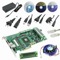
Board, Cables, CD, DVD, Power Supply
Silicon Manufacturer
Altera
Core Architecture
FPGA
Core Sub-architecture
Arria
Silicon Core Number
EP2
Silicon Family Name
Arria II GX
Rohs Compliant
Yes
For Use With/related Products
EP2AGX125EF35
Lead Free Status / RoHS Status
Lead free / RoHS Compliant
Other names
544-2600
Available stocks
Company
Part Number
Manufacturer
Quantity
Price
Company:

Part Number:
DK-DEV-2AGX125N
Manufacturer:
Altera
Quantity:
135


Chapter 2: Board Components
Clock Circuitry
Clock Circuitry
Figure 2–6. Arria II GX FPGA Development Board Clock Inputs
Table 2–20. Arria II GX FPGA Development Board Clock Inputs (Part 1 of 2)
February 2011 Altera Corporation
U25
3 .3 V
Source
Arria II GX FPGA Clock Inputs
Control signals route
CLK 2 _ RSTn
CLK 2 _ OS 1
to MAX II
CLK 2 _ OS 0
CLK 2 _ CE
7 6 5 4 3 2 1 0
CLK 2 _ PR 1
CLK 2 _ PR 0
CLK 2 _ OD 2
CLK 2 _ OD 1
CLK 2 _ OD 0
SMA
Schematic Signal Name
This section describes the board's clock inputs and outputs.
The development board has two types of clock inputs—global clock inputs and
transceiver reference clock inputs.
Figure 2–6
Table 2–20
board.
CLOCK_SMA
CLK_155_P
CLK_155_N
CDCM61004RHB
(Default 125 MHz)
Low Jitter Clock
Generator*
155.52 M
HSMA CLK_IN_P[2]/N[2]
25 MHz
shows the Arria II GX FPGA development board clock inputs.
Crystal
shows the external clock inputs for the Arria II GX FPGA development
(LVPECL)
XIN 2
PLL 2
PLL 1
Q 3
6 B
(LVDS)
EP2AGX125EF35
(LVDS)
(LVDS)
6 A
Q 2
* CDCM6100x can be set to output frequencies
PLL
of 100 MHz, 125 MHz, 156.25 MHz.
R29
R30
Pin
5
PLL
Q 1
5 A
6
7 6 5 4 3 2 1 0
ENET_RX_CLK
I/O Standard
PLL 3
PLL 4
(2.5 V)
LVPECL
Q 0
5 B
CLK_SEL
(LVDS)
REFCLK INPUT
SMA
(LVPECL )
(LVDS)
155.52 MHz oscillator which drives the
transceiver Q2 reference clock input with
100 OCT.
Arria II GX FPGA Development Board Reference Manual
2-to-4 buffer
SMA
HSMB_CLK_IN0
HSMA_CLK_IN0
XIN 1
25 MHz
Crystal
(Default 100 MHz)
CDCM61001RHB
3 .3 V
Low Jitter Clock
Generator*
EPM2210 System Controller
Description
MAX II CPLD
50 M
(2.5 V)
100 M
(2.5 V)
3 .3 V
2–21
Related parts for DK-DEV-2AGX125N
Image
Part Number
Description
Manufacturer
Datasheet
Request
R

Part Number:
Description:
KIT DEV CYCLONE III LS EP3CLS200
Manufacturer:
Altera
Datasheet:

Part Number:
Description:
KIT DEV STRATIX IV FPGA 4SE530
Manufacturer:
Altera
Datasheet:

Part Number:
Description:
KIT DEV FPGA 2AGX260 W/6.375G TX
Manufacturer:
Altera
Datasheet:

Part Number:
Description:
KIT DEV MAX V 5M570Z
Manufacturer:
Altera
Datasheet:

Part Number:
Description:
KIT DEV STRATIX V FPGA 5SGXEA7
Manufacturer:
Altera
Datasheet:

Part Number:
Description:
KIT DEVELOPMENT STRATIX III
Manufacturer:
Altera
Datasheet:

Part Number:
Description:
KIT DEVELOPMENT STRATIX IV
Manufacturer:
Altera
Datasheet:

Part Number:
Description:
KIT DEV ARRIA GX 1AGX60N
Manufacturer:
Altera
Datasheet:
Part Number:
Description:
KIT STARTER CYCLONE IV GX
Manufacturer:
Altera
Datasheet:
Part Number:
Description:
KIT DEVELOPMENT STRATIX IV
Manufacturer:
Altera
Datasheet:

Part Number:
Description:
CPLD, EP610 Family, ECMOS Process, 300 Gates, 16 Macro Cells, 16 Reg., 16 User I/Os, 5V Supply, 35 Speed Grade, 24DIP
Manufacturer:
Altera Corporation
Datasheet:
Part Number:
Description:
CPLD, EP610 Family, ECMOS Process, 300 Gates, 16 Macro Cells, 16 Reg., 16 User I/Os, 5V Supply, 15 Speed Grade, 24DIP
Manufacturer:
Altera Corporation
Datasheet: