DK-DEV-2AGX125N Altera, DK-DEV-2AGX125N Datasheet
DK-DEV-2AGX125N
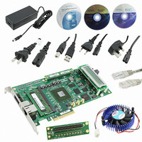
Specifications of DK-DEV-2AGX125N
Available stocks


Related parts for DK-DEV-2AGX125N


DK-DEV-2AGX125N Summary of contents
Page 1
... Arria II GX FPGA Development Kit User Guide 101 Innovation Drive San Jose, CA 95134 www.altera.com UG-01066-1.1 Arria II GX FPGA Development Kit User Guide Subscribe ...
Page 2
... Altera warrants performance of its semiconductor products to current specifications in accordance with Altera's standard warranty, but reserves the right to make changes to any products and services at any time without notice. Altera assumes no responsibility or liability arising out of the application or use of any information, product, or service described herein except as expressly agreed to in writing by Altera. Altera customers are advised to obtain the latest version of device specifications before relying on any published information and before placing orders for products or services ...
Page 3
... LCD . . . . . . . . . . . . . . . . . . . . . . . . . . . . . . . . . . . . . . . . . . . . . . . . . . . . . . . . . . . . . . . . . . . . . . . . . . . . . . 6–7 User Dipswitch . . . . . . . . . . . . . . . . . . . . . . . . . . . . . . . . . . . . . . . . . . . . . . . . . . . . . . . . . . . . . . . . . . . . . 6–7 User LEDs . . . . . . . . . . . . . . . . . . . . . . . . . . . . . . . . . . . . . . . . . . . . . . . . . . . . . . . . . . . . . . . . . . . . . . . . . 6–8 Pushbutton Switches . . . . . . . . . . . . . . . . . . . . . . . . . . . . . . . . . . . . . . . . . . . . . . . . . . . . . . . . . . . . . . . . 6–8 The Flash Tab . . . . . . . . . . . . . . . . . . . . . . . . . . . . . . . . . . . . . . . . . . . . . . . . . . . . . . . . . . . . . . . . . . . . . . . . 6–8 Read . . . . . . . . . . . . . . . . . . . . . . . . . . . . . . . . . . . . . . . . . . . . . . . . . . . . . . . . . . . . . . . . . . . . . . . . . . . . . . 6–9 Write . . . . . . . . . . . . . . . . . . . . . . . . . . . . . . . . . . . . . . . . . . . . . . . . . . . . . . . . . . . . . . . . . . . . . . . . . . . . . 6–9 Random Test . . . . . . . . . . . . . . . . . . . . . . . . . . . . . . . . . . . . . . . . . . . . . . . . . . . . . . . . . . . . . . . . . . . . . . . 6–9 CFI Query . . . . . . . . . . . . . . . . . . . . . . . . . . . . . . . . . . . . . . . . . . . . . . . . . . . . . . . . . . . . . . . . . . . . . . . . . 6–9 Increment Test . . . . . . . . . . . . . . . . . . . . . . . . . . . . . . . . . . . . . . . . . . . . . . . . . . . . . . . . . . . . . . . . . . . . . 6–9 Reset . . . . . . . . . . . . . . . . . . . . . . . . . . . . . . . . . . . . . . . . . . . . . . . . . . . . . . . . . . . . . . . . . . . . . . . . . . . . . . 6–9 February 2011 Altera Corporation Contents Arria II GX FPGA Development Kit User Guide ...
Page 4
... Programming Flash Memory Using the Nios II EDS . . . . . . . . . . . . . . . . . . . . . . . . . . . . . . . . . . . . . . . . . A–3 Restoring the Flash Device to the Factory Settings . . . . . . . . . . . . . . . . . . . . . . . . . . . . . . . . . . . . . . . . . . A–4 Restoring the MAX II CPLD to the Factory Settings . . . . . . . . . . . . . . . . . . . . . . . . . . . . . . . . . . . . . . . . . A–5 Additional Information Document Revision History . . . . . . . . . . . . . . . . . . . . . . . . . . . . . . . . . . . . . . . . . . . . . . . . . . . . . . . . . . . Info–1 How to Contact Altera . . . . . . . . . . . . . . . . . . . . . . . . . . . . . . . . . . . . . . . . . . . . . . . . . . . . . . . . . . . . . . . . Info–1 Arria II GX FPGA Development Kit User Guide Contents February 2011 Altera Corporation ...
Page 5
... Contents Typographic Conventions . . . . . . . . . . . . . . . . . . . . . . . . . . . . . . . . . . . . . . . . . . . . . . . . . . . . . . . . . . . . . Info–1 February 2011 Altera Corporation v Arria II GX FPGA Development Kit User Guide ...
Page 6
... Arria II GX FPGA Development Kit User Guide Contents February 2011 Altera Corporation ...
Page 7
... LEDs to the remaining 40 CMOS signals Software The software for this kit, described in the following sections, is available on the Altera website for immediate downloading. You can also request to have Altera mail the software to you on DVDs. February 2011 Altera Corporation ® ...
Page 8
... Quartus II Subscription Edition Software The Quartus II Subscription Edition Software is a licensed set of Altera tools with full functionality. Your kit includes a one-year license for the Quartus II software (Windows platform only). This license entitles you to all the features of the subscription edition for a period of one year. After the year, you must purchase a renewal subscription to continue using the software ...
Page 9
... Before using the kit or installing the software, check the kit contents and inspect the board to verify that you received all of the items listed in If any of the items are missing, contact Altera before you proceed. Inspect the Board To inspect the board, perform the following steps: 1 ...
Page 10
... References Use the following links to check the Altera website for other related information: ■ For the latest board design files and reference designs, refer to the FPGA Development Kit For additional daughter cards available for purchase, refer to the ■ Board Daughtercards ■ ...
Page 11
... MegaCore IP Library. The Quartus II software (including SOPC Builder) and the Nios II EDS are the primary FPGA development tools used to create the reference designs in this kit. To install the Altera development tools, perform the following steps: 1. Run the Quartus II Subscription Edition Software installer you acquired in “ ...
Page 12
... NIC ID. Your NIC ID is the 12-digit hexadecimal number on the Physical Address line. 4. When licensing is complete, Altera emails a license.dat file to you. Store the file on your computer and use the License Setup page of the Options dialog box in the Quartus II software to enable the software ...
Page 13
... USB-Blaster driver on the host computer. f Installation instructions for the USB-Blaster driver for your operating system are available on the Altera website. On the the Altera website, locate the table entry for your configuration and click the link to access the instructions. February 2011 Altera Corporation Figure 3– ...
Page 14
... Arria II GX FPGA Development Kit User Guide Chapter 3: Software Installation Installing the USB-Blaster Driver February 2011 Altera Corporation ...
Page 15
... When configuration is complete, the CONF DONE LED (D14) illuminates, signaling that the Arria II GX device configured successfully. f For more information about the PFL megafunction, refer to Megafunction User February 2011 Altera Corporation 4. Development Board Setup Guide. to return the board to its factory Figure 4–1 ...
Page 16
... User DIP Switch OFF = SW2 PCIe MODE DIP Switch SW3 Table 4–1 and Function Chapter 4: Development Board Setup Factory Default Switch Settings Board Settings DIP Switch OFF = SW4 Figure 4–1. Default Position — February 2011 Altera Corporation ...
Page 17
... This jumper has the following options: J9 pins 3-4 HSMA DIS Installing the shunt removes HSMC port A from the JTAG chain. ■ Removing the shunt includes HSMC port A in the JTAG chain. ■ February 2011 Altera Corporation Table 4–2 and Figure 4–1. Function Table 4–3 ...
Page 18
... For more information about the FPGA board settings, refer to the Development Board Reference Arria II GX FPGA Development Kit User Guide Chapter 4: Development Board Setup Function Manual. February 2011 Altera Corporation Factory Default Switch Settings Default Shunt Position Installed Installed Arria II GX FPGA ...
Page 19
... The web page allows you to upload new FPGA designs to the user hardware portion of flash memory, and provides links to useful information on the Altera website, including kit-specific links and design resources. ...
Page 20
... Board Update Portal web page the Hardware File Name field specify the .flash file that you either downloaded from the Altera website or created on your own. If there is a software component to the design, specify it in the same manner using the Software File Name field, otherwise leave the Software File Name field blank ...
Page 21
... The application allows you to exercise most of the board components. While using the application, you reconfigure the FPGA several times with test designs specific to the functionality you are testing. February 2011 Altera Corporation 6. Board Test System 3–2. Arria II GX FPGA Development Kit User Guide ...
Page 22
... JTAG bus to the MAX II device, you can measure the power of any design in the FPGA, including your own designs. Arria II GX FPGA Development Kit User Guide Figure 6–1 shows the initial GUI for a board that is in the Chapter 6: Board Test System February 2011 Altera Corporation ...
Page 23
... BoardTestSystem.exe application Windows, click Start > All Programs > Altera > Arria II GX FPGA Development Kit <version> > Board Test System to run the application. A GUI appears, displaying the application tab that corresponds to the design running in the FPGA. The Arria II GX FPGA development board’s flash memory ships preconfigured with the design that corresponds to the Config, GPIO, and SSRAM, and Flash tabs ...
Page 24
... The following sections describe the controls on the Config tab. Arria II GX FPGA Development Kit User Guide shows the Config tab. The tab displays the contents of the Chapter 6: Board Test System Using the Board Test System February 2011 Altera Corporation ...
Page 25
... Use PSR—Allows the PSR to determine the page of flash memory to use for ■ FPGA reconfiguration. Use PSS—Allows the PSS to determine the page of flash memory to use for ■ FPGA reconfiguration. February 2011 Altera Corporation Table 6–1. Changes to the register values with the GUI Read/Write Capability Write only Set initiate an FPGA reconfiguration ...
Page 26
... Arria II GX FPGA Development Kit User Guide Chapter 6: Board Test System Using the Board Test System Table 6–1 Table 6–1 for the list of available Table 6–1 for more information. Arria II GX FPGA Development Kit February 2011 Altera Corporation Table 6–1 for the list of page of the ...
Page 27
... This read-only control displays the current positions of the switches in the user DIP switch bank (SW2). Change the switches on the board to see the graphical display change accordingly. February 2011 Altera Corporation Figure 6–3 shows the GPIO tab. Arria II GX FPGA Development Kit User Guide ...
Page 28
... The Flash tab allows you to read and write flash memory on your board. shows the Flash tab. Figure 6–4. The Flash Tab The following sections describe the controls on the Flash tab. Arria II GX FPGA Development Kit User Guide Chapter 6: Board Test System Using the Board Test System Figure 6–4 February 2011 Altera Corporation ...
Page 29
... Flash tab. Erase Erases flash memory. Limited to scratch page in the upper 128K blocks. Flash Memory Map Displays the flash memory map for the Arria II GX FPGA Development Kit. February 2011 Altera Corporation Table A–1 on page A–1). 6–9 Figure 6–1 on ...
Page 30
... If you enter an address outside of the 0x0000.0000 to 0x001F.FFFF SRAM address space, a warning message identifies the valid SRAM address range. Arria II GX FPGA Development Kit User Guide shows the SSRAM tab. Chapter 6: Board Test System Using the Board Test System February 2011 Altera Corporation ...
Page 31
... Starts an incrementing data pattern test to flash memory. The DDR3 Tab The DDR3 tab allows you to read and write the DDR3 memory on your board. Figure 6–6 shows the DDR3 tab. Figure 6–6. The DDR3 Tab February 2011 Altera Corporation 6–11 Arria II GX FPGA Development Kit User Guide ...
Page 32
... PRBS—Selects pseudo-random bit sequences. ■ 1 Frequency rates for production silicon speed grade C4N only. Arria II GX FPGA Development Kit User Guide Chapter 6: Board Test System Using the Board Test System 1 February 2011 Altera Corporation ...
Page 33
... Write Only—Selects write transactions for analysis. The DDR2 Tab The DDR2 tab allows you to read and write the DDR2 memory on your board. Figure 6–7 shows the DDR2 tab. Figure 6–7. The DDR2 Tab February 2011 Altera Corporation 6–13 Arria II GX FPGA Development Kit User Guide ...
Page 34
... PRBS—Selects pseudo-random bit sequences. ■ 1 Frequency rates for production silicon speed grade C4N only. Arria II GX FPGA Development Kit User Guide Chapter 6: Board Test System Using the Board Test System 1 February 2011 Altera Corporation ...
Page 35
... Write Only—Selects write transactions for analysis. The HSMC Tab The HSMC tab allows you to perform loopback tests on the HSMC port. shows the HSMC tab. Figure 6–8. The HSMC Tab February 2011 Altera Corporation 6–15 Figure 6–8 Arria II GX FPGA Development Kit User Guide ...
Page 36
... This control specifies the type of data contained in the transactions. The following data types are available for analysis: PRBS—Selects pseudo-random bit sequences. ■ Arria II GX FPGA Development Kit User Guide Chapter 6: Board Test System Using the Board Test System Volume 2: Transceivers of the Arria II February 2011 Altera Corporation ...
Page 37
... Gbps, totaling 1.5625 GBps full-duplex. The LVDS SERDES bus is 17 bits wide. The transmit data bus is 16 bits wide and the frequency is 300 MHz double data rate (600 Mbps per pin), equating to a theoretical maximum bandwidth of 1200 MBps. February 2011 Altera Corporation 6–17 Arria II GX FPGA Development Kit User Guide ...
Page 38
... You can also run the Power Monitor as a stand-alone application. PowerTool.exe resides in the <install dir>\kits\arriaIIGX_2agx125_fpga\examples\board_test_system directory. On Windows, click Start > All Programs > Altera > Arria II GX FPGA Development Kit <version> > Power Monitor to start the application. The Power Monitor communicates with the MAX II device on the board through the JTAG bus ...
Page 39
... Update Speed—Specifies how often to refresh the graph. ■ Reset This control clears the graph, resets the minimum and maximum values, and restarts the Power Monitor. February 2011 Altera Corporation Arria II GX FPGA Development Kit Arria II GX FPGA Manual. Arria II GX FPGA Development Kit User Guide 6– ...
Page 40
... JTAG-based applications such as the Board Test System and the Power Monitor to loose their connection to the board. Restart those applications after configuration is complete. Arria II GX FPGA Development Kit User Guide Chapter 6: Board Test System Configuring the FPGA Using the Quartus II Programmer February 2011 Altera Corporation ...
Page 41
... As you develop your own project using the Altera tools, you can program the flash memory device so that your own design loads from flash memory into the FPGA on power up. This appendix describes the preprogrammed contents of the common flash interface (CFI) flash memory device on the Arria II GX FPGA development board and the Nios II EDS tools involved with reprogramming the user portions of the flash memory device ...
Page 42
... Creating Flash Files Using the Nios II EDS If you have an FPGA design developed using the Quartus II software, and software developed using the Nios II EDS, follow these instructions the Windows Start menu, click All Programs > Altera > Nios II EDS > Nios II Command Shell. Arria II GX FPGA Development Kit User Guide ...
Page 43
... FPGA with a flash-writing design. 4. Launch the Quartus II Programmer to configure the FPGA with a .sof capable of flash programming. Refer to Programmer” on page 6–20 February 2011 Altera Corporation “Using the Board Update Portal to Update User for more information. “Configuring the FPGA Using the Quartus II for more information ...
Page 44
... The CONF DONE LED (D14) and the four user LEDs (D7-D10) illuminate indicating that the flash device is ready for programming the Windows Start menu, click All Programs > Altera > Nios II EDS > Nios II Command Shell the Nios II command shell, navigate to the <install dir> ...
Page 45
... The CONF DONE LED (D14) and the four user LEDs (D7-D10) illuminate indicating that the flash device is ready for programming the Windows Start menu, click All Programs > Altera > Nios II EDS > Nios II Command Shell the Nios II command shell, navigate to the <install dir> ...
Page 46
... To ensure that you have the most up-to-date factory restore files and information about this product, refer to the website. Arria II GX FPGA Development Kit User Guide Restoring the MAX II CPLD to the Factory Settings Arria II GX FPGA Development Kit February 2011 Altera Corporation Appendix A page of the Altera ...
Page 47
... Technical training Product literature Non-technical support (General) (Software Licensing) Note to Table: (1) You can also contact your local Altera sales office or sales representative. Typographic Conventions The following table shows the typographic conventions this document uses. Visual Cue Bold Type with Initial Capital ...
Page 48
... A warning calls attention to a condition or possible situation that can cause you injury. The envelope links to the Email Subscription Management Center website, where you can sign up to receive update notifications for Altera documents. Additional Information Typographic Conventions page of the Altera February 2011 Altera Corporation ...