DK-DEV-2AGX125N Altera, DK-DEV-2AGX125N Datasheet - Page 37
DK-DEV-2AGX125N
Manufacturer Part Number
DK-DEV-2AGX125N
Description
KIT DEV ARRIA II GX FPGA 2AGX125
Manufacturer
Altera
Series
Arria II GXr
Type
FPGAr
Datasheets
1.EP2AGX45CU17C6N.pdf
(96 pages)
2.DK-DEV-2AGX125N.pdf
(48 pages)
3.DK-DEV-2AGX125N.pdf
(64 pages)
Specifications of DK-DEV-2AGX125N
Contents
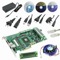
Board, Cables, CD, DVD, Power Supply
Silicon Manufacturer
Altera
Core Architecture
FPGA
Core Sub-architecture
Arria
Silicon Core Number
EP2
Silicon Family Name
Arria II GX
Rohs Compliant
Yes
For Use With/related Products
EP2AGX125EF35
Lead Free Status / RoHS Status
Lead free / RoHS Compliant
Other names
544-2600
Available stocks
Company
Part Number
Manufacturer
Quantity
Price
Company:

Part Number:
DK-DEV-2AGX125N
Manufacturer:
Altera
Quantity:
135


Chapter 2: Board Components
Components and Interfaces
Table 2–34. PCI Express Pin Assignments, Schematic Signal Names, and Functions (Part 1 of 2)
February 2011 Altera Corporation
J14.B14
J14.B15
J14.B19
J14.B20
J14.B23
J14.B24
J14.B27
J14.B28
J14.B33
J14.B34
Board Reference
Add-in card receive bus
Add-in card receive bus
Add-in card receive bus
Add-in card receive bus
Add-in card receive bus
Add-in card receive bus
Add-in card receive bus
Add-in card receive bus
Add-in card receive bus
Add-in card receive bus
The power for the board can be sourced entirely from the PCI Express edge connector
when installed into a PC motherboard. Although the board can also be powered by a
laptop power supply for use on a lab bench, it is not recommended to power from
both supplies at the same time. This board includes ideal diode power sharing devices
to prevent damages or back-current from one supply to the other.
The PCIE_REFCLK_P signal is a 100 MHz differential input that is driven from the PC
motherboard on to this board through the edge connector. This signal connects
directly to a Arria II GX REFCLK input pin pair using DC coupling. This clock is
terminated on the motherboard and therefore, no on-board termination is required.
This clock can have spread-spectrum properties that change its period between
9.847 ps to 10.203 ps. The I/O standard is HCSL.
Figure 2–8
Figure 2–8. PCI Express Reference Clock Levels
The JTAG and SMB are optional signals in the PCI Express specification. Both types of
signals are wired to the Arria II GX device but are not required for normal operation.
The PCI Express control DIP switch allows the presence detect grounding to be
altered to enable a ×1, ×4, or ×8 width edge connector. The PCI Express control DIP
switch does not support auto-negotiation.
Table 2–34
directions are relative to the Arria II GX FPGA.
V
V
CROSS MAX
Description
CROSS MIN
shows the PCI Express reference clock levels.
summarizes the PCI Express pin assignments. The signal names and
V
V
MAX
MIN
REFCLK –
REFCLK +
= 550 mV
= 250 mV
= 1.15 V
= –0.30 V
Schematic Signal
PCIE_RX_P0
PCIE_RX_N0
PCIE_RX_P1
PCIE_RX_N1
PCIE_RX_P2
PCIE_RX_N2
PCIE_RX_P3
PCIE_RX_N3
PCIE_RX_P4
PCIE_RX_N4
Name
Arria II GX FPGA Development Board Reference Manual
I/O Standard
1.5-V PCML
Arria II GX Device
Pin Number
AN33
AN34
AG33
AG34
AL33
AL34
AJ33
AJ34
AE33
AE34
2–29
Related parts for DK-DEV-2AGX125N
Image
Part Number
Description
Manufacturer
Datasheet
Request
R

Part Number:
Description:
KIT DEV CYCLONE III LS EP3CLS200
Manufacturer:
Altera
Datasheet:

Part Number:
Description:
KIT DEV STRATIX IV FPGA 4SE530
Manufacturer:
Altera
Datasheet:

Part Number:
Description:
KIT DEV FPGA 2AGX260 W/6.375G TX
Manufacturer:
Altera
Datasheet:

Part Number:
Description:
KIT DEV MAX V 5M570Z
Manufacturer:
Altera
Datasheet:

Part Number:
Description:
KIT DEV STRATIX V FPGA 5SGXEA7
Manufacturer:
Altera
Datasheet:

Part Number:
Description:
KIT DEVELOPMENT STRATIX III
Manufacturer:
Altera
Datasheet:

Part Number:
Description:
KIT DEVELOPMENT STRATIX IV
Manufacturer:
Altera
Datasheet:

Part Number:
Description:
KIT DEV ARRIA GX 1AGX60N
Manufacturer:
Altera
Datasheet:
Part Number:
Description:
KIT STARTER CYCLONE IV GX
Manufacturer:
Altera
Datasheet:
Part Number:
Description:
KIT DEVELOPMENT STRATIX IV
Manufacturer:
Altera
Datasheet:

Part Number:
Description:
CPLD, EP610 Family, ECMOS Process, 300 Gates, 16 Macro Cells, 16 Reg., 16 User I/Os, 5V Supply, 35 Speed Grade, 24DIP
Manufacturer:
Altera Corporation
Datasheet:
Part Number:
Description:
CPLD, EP610 Family, ECMOS Process, 300 Gates, 16 Macro Cells, 16 Reg., 16 User I/Os, 5V Supply, 15 Speed Grade, 24DIP
Manufacturer:
Altera Corporation
Datasheet: