DK-DEV-2AGX125N Altera, DK-DEV-2AGX125N Datasheet - Page 53
DK-DEV-2AGX125N
Manufacturer Part Number
DK-DEV-2AGX125N
Description
KIT DEV ARRIA II GX FPGA 2AGX125
Manufacturer
Altera
Series
Arria II GXr
Type
FPGAr
Datasheets
1.EP2AGX45CU17C6N.pdf
(96 pages)
2.DK-DEV-2AGX125N.pdf
(48 pages)
3.DK-DEV-2AGX125N.pdf
(64 pages)
Specifications of DK-DEV-2AGX125N
Contents
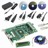
Board, Cables, CD, DVD, Power Supply
Silicon Manufacturer
Altera
Core Architecture
FPGA
Core Sub-architecture
Arria
Silicon Core Number
EP2
Silicon Family Name
Arria II GX
Rohs Compliant
Yes
For Use With/related Products
EP2AGX125EF35
Lead Free Status / RoHS Status
Lead free / RoHS Compliant
Other names
544-2600
Available stocks
Company
Part Number
Manufacturer
Quantity
Price
Company:

Part Number:
DK-DEV-2AGX125N
Manufacturer:
Altera
Quantity:
135


Chapter 2: Board Components
Memory
Table 2–42. DDR2 SODIMM Pin Assignments, Signal Names and Functions (Part 4 of 4)
Table 2–43. DDR2 SODIMM Component References and Manufacturing Information
Table 2–44. SSRAM Pin Assignments, Schematic Signal Names, and Functions (Part 1 of 3)
February 2011 Altera Corporation
J7.167
J7.179
J7.181
J7.189
J7.191
J7.180
J7.182
J7.192
J7.194
J7.185
J7.188
J7.186
J7
Module
U22.R6
U22.P6
U22.A2
Board Reference
Board Reference
Reference
Board
SSRAM
200-pin DDR2 SODIMM socket
128 M × 8 banks, 400M, CL6
Address bus
Address bus
Address bus
Data strobe N byte lane 6
Data bus byte lane 7
Data bus byte lane 7
Data bus byte lane 7
Data bus byte lane 7
Data bus byte lane 7
Data bus byte lane 7
Data bus byte lane 7
Data bus byte lane 7
Write mask byte lane 7
Data strobe P byte lane 7
Data strobe N byte lane 7
Table 2–43
information.
The SSRAM device consists of a single standard synchronous SRAM, providing 2 MB
of memory with a 36-bit data bus. This device is part of the shared FSM bus which
connects to the flash memory, SRAM, and MAX II CPLD EPM2210 System Controller.
The device speed is 200 MHz single-data-rate. There is no minimum speed for this
device. The theoretical bandwidth of this 32-bit memory interface is 6.4 Gbps for
continuous bursts. The read latency for any address is two clocks, in which at
200 MHz, the latency is 10 ns and at 50 MHz, the latency is 40 ns. The write latency is
one clock.
Table 2–44
names and types are relative to the Arria II GX device in terms of I/O setting and
direction.
Description
Description
Description
lists the DDR2 SODIMM component references and manufacturing
lists the SSRAM pin assignments, signal names, and functions. The signal
Tyco Electronics
Micron
Manufacturer
Schematic Signal Name
Schematic Signal
DDR2_DQSN6
DDR2_DQSN7
FSM_A2
FSM_A3
FSM_A4
DDR2_DQ56
DDR2_DQ57
DDR2_DQ58
DDR2_DQ59
DDR2_DQ60
DDR2_DQ61
DDR2_DQ62
DDR2_DQ63
DDR2_DQS7
DDR2_DM7
Name
MT8HTF12864HY-800G1
Manufacturing
Part Number
1-1734075-1
Arria II GX FPGA Development Board Reference Manual
I/O Standard
1.8-V SSTL Class I
2.5-V
I/O Standard
www.tycoelectronics.com
www.micron.com
Arria II GX Device
Manufacturer
Pin Number
Website
Pin Number
D29
Arria II GX
J21
L13
Device
AM10
AL12
AF15
AJ12
AJ16
AE15
AM7
AM8
AP2
AN9
AP3
AN4
2–45
Related parts for DK-DEV-2AGX125N
Image
Part Number
Description
Manufacturer
Datasheet
Request
R

Part Number:
Description:
KIT DEV CYCLONE III LS EP3CLS200
Manufacturer:
Altera
Datasheet:

Part Number:
Description:
KIT DEV STRATIX IV FPGA 4SE530
Manufacturer:
Altera
Datasheet:

Part Number:
Description:
KIT DEV FPGA 2AGX260 W/6.375G TX
Manufacturer:
Altera
Datasheet:

Part Number:
Description:
KIT DEV MAX V 5M570Z
Manufacturer:
Altera
Datasheet:

Part Number:
Description:
KIT DEV STRATIX V FPGA 5SGXEA7
Manufacturer:
Altera
Datasheet:

Part Number:
Description:
KIT DEVELOPMENT STRATIX III
Manufacturer:
Altera
Datasheet:

Part Number:
Description:
KIT DEVELOPMENT STRATIX IV
Manufacturer:
Altera
Datasheet:

Part Number:
Description:
KIT DEV ARRIA GX 1AGX60N
Manufacturer:
Altera
Datasheet:
Part Number:
Description:
KIT STARTER CYCLONE IV GX
Manufacturer:
Altera
Datasheet:
Part Number:
Description:
KIT DEVELOPMENT STRATIX IV
Manufacturer:
Altera
Datasheet:

Part Number:
Description:
CPLD, EP610 Family, ECMOS Process, 300 Gates, 16 Macro Cells, 16 Reg., 16 User I/Os, 5V Supply, 35 Speed Grade, 24DIP
Manufacturer:
Altera Corporation
Datasheet:
Part Number:
Description:
CPLD, EP610 Family, ECMOS Process, 300 Gates, 16 Macro Cells, 16 Reg., 16 User I/Os, 5V Supply, 15 Speed Grade, 24DIP
Manufacturer:
Altera Corporation
Datasheet: