DK-DEV-2AGX125N Altera, DK-DEV-2AGX125N Datasheet - Page 59
DK-DEV-2AGX125N
Manufacturer Part Number
DK-DEV-2AGX125N
Description
KIT DEV ARRIA II GX FPGA 2AGX125
Manufacturer
Altera
Series
Arria II GXr
Type
FPGAr
Datasheets
1.EP2AGX45CU17C6N.pdf
(96 pages)
2.DK-DEV-2AGX125N.pdf
(48 pages)
3.DK-DEV-2AGX125N.pdf
(64 pages)
Specifications of DK-DEV-2AGX125N
Contents
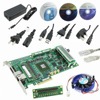
Board, Cables, CD, DVD, Power Supply
Silicon Manufacturer
Altera
Core Architecture
FPGA
Core Sub-architecture
Arria
Silicon Core Number
EP2
Silicon Family Name
Arria II GX
Rohs Compliant
Yes
For Use With/related Products
EP2AGX125EF35
Lead Free Status / RoHS Status
Lead free / RoHS Compliant
Other names
544-2600
Available stocks
Company
Part Number
Manufacturer
Quantity
Price
Company:

Part Number:
DK-DEV-2AGX125N
Manufacturer:
Altera
Quantity:
135


Chapter 2: Board Components
Power Supply
Figure 2–12. Power Measurement Circuit
Table 2–48. Power Rails Measurement Based on the Rotary Switch Position (Part 1 of 2)
February 2011 Altera Corporation
0
1
2
3
4
5
6
7
Switch
Supply
Supply
#0
#13
Power Measurement
Schematic Signal Name
A2VCCIO_B3B_B5B_B6B
A2VCCIO_B7B_B8A
A2VCCIO_B3A_B4
A2VCCIO_B5A
A2VCCIO_B6A
A2VCCIO_B7A
A2VCCH_GXB
Feedback
A2VCCPD
There are 14 power supply rails which have on-board voltage and current sense
capabilities. These 8-channel differential 24-bit ADC devices and rails are split from
the primary supply plane by a low-value sense resistor for the ADC to measure
voltage and current. An SPI bus connects these ADC devices to the MAX II CPLD
EPM2210 System Controller as well as the Arria II GX FPGA.
Figure 2–12
Table 2–48
measured and the device pin specifies the devices attached to the rail. If no subsignal
is named, the power is the total output power for that voltage.
R
SENSE
Feedback
lists the targeted rails. The signal name specifies the name of the rail being
R
shows the block diagram for the power measurement circuitry.
SENSE
Voltage (V)
Power Supply Load #0
Power Supply Load #13
2.5
2.5
2.5
2.5
2.5
1.8
1.5
1.5
U16
U11
8 Ch.
8 Ch.
LTC2418
DSO
DSO
SCK
SCK
CSn
CSn
DSI
DSI
VCCIO_B3B
VCCIO_B5B
VCCIO_B7B
VCCIO_B5A
VCCIO_B6A
VCCIO_B7B
VCCIO_B8A
VCCIO_B3A
VCCIO_B7A
VCCH_GXB
Device Pin
VCCIO_B4
VCCPD
USB-Blaster
Embedded
Bank 3B I/O power (HSMB)
Bank 5B I/O power (HSMB)
Bank 7B I/O power (HSMB)
Bank 5A I/O power (FSM, flash)
Bank 6A I/O power (SSRAM, MAX II, user I/O)
Bank 7B I/O power (HSMA)
Bank 8A I/O power (HSMA)
Bank 3A I/O power (DDR2 SODIMM)
Bank 4 I/O power (DDR2 SODIMM)
Bank 7A I/O power (DDR3)
I/O pre-drivers and input buffers
XCVR output (TX) buffer
Arria II GX FPGA Development Board Reference Manual
EPM
240
EPM2210
Z
JTAG Chain
USB
PHY
Description
2AGX125
To User PC
Power GUI
RS
D(0:7)
E
RW
2x16 LCD
14-pin
2–51
Related parts for DK-DEV-2AGX125N
Image
Part Number
Description
Manufacturer
Datasheet
Request
R

Part Number:
Description:
KIT DEV CYCLONE III LS EP3CLS200
Manufacturer:
Altera
Datasheet:

Part Number:
Description:
KIT DEV STRATIX IV FPGA 4SE530
Manufacturer:
Altera
Datasheet:

Part Number:
Description:
KIT DEV FPGA 2AGX260 W/6.375G TX
Manufacturer:
Altera
Datasheet:

Part Number:
Description:
KIT DEV MAX V 5M570Z
Manufacturer:
Altera
Datasheet:

Part Number:
Description:
KIT DEV STRATIX V FPGA 5SGXEA7
Manufacturer:
Altera
Datasheet:

Part Number:
Description:
KIT DEVELOPMENT STRATIX III
Manufacturer:
Altera
Datasheet:

Part Number:
Description:
KIT DEVELOPMENT STRATIX IV
Manufacturer:
Altera
Datasheet:

Part Number:
Description:
KIT DEV ARRIA GX 1AGX60N
Manufacturer:
Altera
Datasheet:
Part Number:
Description:
KIT STARTER CYCLONE IV GX
Manufacturer:
Altera
Datasheet:
Part Number:
Description:
KIT DEVELOPMENT STRATIX IV
Manufacturer:
Altera
Datasheet:

Part Number:
Description:
CPLD, EP610 Family, ECMOS Process, 300 Gates, 16 Macro Cells, 16 Reg., 16 User I/Os, 5V Supply, 35 Speed Grade, 24DIP
Manufacturer:
Altera Corporation
Datasheet:
Part Number:
Description:
CPLD, EP610 Family, ECMOS Process, 300 Gates, 16 Macro Cells, 16 Reg., 16 User I/Os, 5V Supply, 15 Speed Grade, 24DIP
Manufacturer:
Altera Corporation
Datasheet: