DK-DEV-2AGX125N Altera, DK-DEV-2AGX125N Datasheet - Page 10
DK-DEV-2AGX125N
Manufacturer Part Number
DK-DEV-2AGX125N
Description
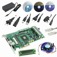
KIT DEV ARRIA II GX FPGA 2AGX125
Manufacturer
Altera
Series
Arria II GXr
Type
FPGAr
Datasheets
1.EP2AGX45CU17C6N.pdf
(96 pages)
2.DK-DEV-2AGX125N.pdf
(48 pages)
3.DK-DEV-2AGX125N.pdf
(64 pages)
Specifications of DK-DEV-2AGX125N
Contents
Board, Cables, CD, DVD, Power Supply
Silicon Manufacturer
Altera
Core Architecture
FPGA
Core Sub-architecture
Arria
Silicon Core Number
EP2
Silicon Family Name
Arria II GX
Rohs Compliant
Yes
For Use With/related Products
EP2AGX125EF35
Lead Free Status / RoHS Status
Lead free / RoHS Compliant
Other names
544-2600
Available stocks
Company
Part Number
Manufacturer
Quantity
Price
Company:

Part Number:
DK-DEV-2AGX125N
Manufacturer:
Altera
Quantity:
135


2–2
Board Overview
Figure 2–1. Overview of the Arria II GX FPGA Development Board Features
Table 2–1. Arria II GX FPGA Development Board Components (Part 1 of 3)
Arria II GX FPGA Development Board Reference Manual
Featured Devices
U19
U32
Configuration, Status, and Setup Elements
J6
J9
SW4
J5
SW3
D14
JTAG Connector
Gigabit Ethernet
Board Reference
DDR2 SODIMM
Connector (J6)
General User
Push-buttons
USB Type-B
JTAG Chain
Header (J9)
(PB1, PB2)
Switches
Port (J8)
(J5)
(J7)
FPGA
CPLD
USB type-B connector
JTAG chain header
Board settings DIP switch
JTAG connector
PCI Express DIP switch
Configuration done LED
CPU Reset Push-button Switch (PB3)
This section provides an overview of the Arria II GX FPGA development board,
including an annotated board image and component descriptions.
provides an overview of the development board features.
Table 2–1
HSMC Port B (J1)
Arria II GX
FPGA
(U19)
User LEDs (D7-D10)
Type
describes the components and lists their corresponding board references.
Connector
Express
Edge
(J14)
PCI
Express
(SW3)
Mode
PCI
Set
(D24-D26)
Express
Status
Mode
EP2AGX125EF35, 1152-pin FBGA.
EPM2210F256, 256-pin FBGA.
Connects to the computer to enable embedded USB-Blaster JTAG.
Jumper shunts which enables and disables devices in the JTAG chain.
Controls the MAX II CPLD EPM2210 System Controller functions such
as clock enable, SMA clock input control, and which image to load
from flash memory at power-up.
Disables the embedded blaster (for use with external USB-Blasters).
Controls the PCI Express lane width by connecting prsnt pins
together on the PCI Express edge connector.
Illuminates when the FPGA is configured.
PCI
User DIP Switch (SW2)
Max II Reset Push-Button Switch (PB4)
Clock Input
Connector
(J10, J11)
SMA
HSMC Port A (J2)
Connector
Output
Clock
(J12)
SMA
EPM2210
Controller
System
MAX II
CPLD
(U32)
DIP Switch
Settings
Description
(SW4)
Board
Configuration LEDs (D11-D16)
Load Image (PB5), Image Select Push-button Switch (PB6)
February 2011 Altera Corporation
Chapter 2: Board Components
Figure 2–1
Board Overview
Flash x16
Memory (U23)
DDR3 x16 (U13)
SSRAM x36
Memory (U22)
Fan Power (J13)
Power Switch (SW1)
DC Input Jack (J4)
Character LCD (J3)
Related parts for DK-DEV-2AGX125N
Image
Part Number
Description
Manufacturer
Datasheet
Request
R

Part Number:
Description:
KIT DEV CYCLONE III LS EP3CLS200
Manufacturer:
Altera
Datasheet:

Part Number:
Description:
KIT DEV STRATIX IV FPGA 4SE530
Manufacturer:
Altera
Datasheet:

Part Number:
Description:
KIT DEV FPGA 2AGX260 W/6.375G TX
Manufacturer:
Altera
Datasheet:

Part Number:
Description:
KIT DEV MAX V 5M570Z
Manufacturer:
Altera
Datasheet:

Part Number:
Description:
KIT DEV STRATIX V FPGA 5SGXEA7
Manufacturer:
Altera
Datasheet:

Part Number:
Description:
KIT DEVELOPMENT STRATIX III
Manufacturer:
Altera
Datasheet:

Part Number:
Description:
KIT DEVELOPMENT STRATIX IV
Manufacturer:
Altera
Datasheet:

Part Number:
Description:
KIT DEV ARRIA GX 1AGX60N
Manufacturer:
Altera
Datasheet:
Part Number:
Description:
KIT STARTER CYCLONE IV GX
Manufacturer:
Altera
Datasheet:
Part Number:
Description:
KIT DEVELOPMENT STRATIX IV
Manufacturer:
Altera
Datasheet:

Part Number:
Description:
CPLD, EP610 Family, ECMOS Process, 300 Gates, 16 Macro Cells, 16 Reg., 16 User I/Os, 5V Supply, 35 Speed Grade, 24DIP
Manufacturer:
Altera Corporation
Datasheet:
Part Number:
Description:
CPLD, EP610 Family, ECMOS Process, 300 Gates, 16 Macro Cells, 16 Reg., 16 User I/Os, 5V Supply, 15 Speed Grade, 24DIP
Manufacturer:
Altera Corporation
Datasheet: