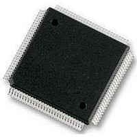
S9S12XS128J1MAL Freescale Semiconductor, S9S12XS128J1MAL Datasheet - Page 611

S9S12XS128J1MAL
Manufacturer Part Number
S9S12XS128J1MAL
Description
IC MCU 16BIT 128KB FLSH 112LQFP
Manufacturer
Freescale Semiconductor
Series
HCS12r
Datasheet
1.MC9S12XS64CAE.pdf
(738 pages)
Specifications of S9S12XS128J1MAL
Core Processor
HCS12X
Core Size
16-Bit
Speed
40MHz
Connectivity
CAN, SCI, SPI
Peripherals
LVD, POR, PWM, WDT
Number Of I /o
91
Program Memory Size
128KB (128K x 8)
Program Memory Type
FLASH
Eeprom Size
8K x 8
Ram Size
8K x 8
Voltage - Supply (vcc/vdd)
1.72 V ~ 5.5 V
Data Converters
A/D 16x12b
Oscillator Type
External
Operating Temperature
-40°C ~ 125°C
Package / Case
112-LQFP
Processor Series
S12XS
Core
HCS12
Data Bus Width
16 bit
Data Ram Size
8 KB
Interface Type
CAN, SCI, SPI
Maximum Clock Frequency
40 MHz
Number Of Programmable I/os
91
Number Of Timers
12
Maximum Operating Temperature
+ 125 C
Mounting Style
SMD/SMT
3rd Party Development Tools
EWHCS12
Development Tools By Supplier
DEMO9S12XSFAME, EVB9S12XEP100
Minimum Operating Temperature
- 40 C
On-chip Adc
12 bit, 16 Channel
Lead Free Status / RoHS Status
Lead free / RoHS Compliant
Available stocks
Company
Part Number
Manufacturer
Quantity
Price
Company:
Part Number:
S9S12XS128J1MAL
Manufacturer:
Freescale Semiconductor
Quantity:
10 000
- Current page: 611 of 738
- Download datasheet (4Mb)
20.3
This section describes the memory map and registers for the Flash module. Read data from unimplemented
memory space in the Flash module is undefined. Write access to unimplemented or reserved memory space
in the Flash module will be ignored by the Flash module.
20.3.1
The S12X architecture places the P-Flash memory between global addresses 0x7F_0000 and 0x7F_FFFF
as shown in
The FPROT register, described in
accidental program or erase. Three separate memory regions, one growing upward from global address
0x7F_8000 in the Flash memory (called the lower region), one growing downward from global address
0x7F_FFFF in the Flash memory (called the higher region), and the remaining addresses in the Flash
memory, can be activated for protection. The Flash memory addresses covered by these protectable regions
are shown in the P-Flash memory map. The higher address region is mainly targeted to hold the boot loader
code since it covers the vector space. Default protection settings as well as security information that allows
the MCU to restrict access to the Flash module are stored in the Flash configuration field as described in
Table
Freescale Semiconductor
1
0x7F_FF08 – 0x7F_FF0B
0x7F_FF00 – 0x7F_FF07
Older versions may have swapped protection byte addresses
20-3.
Global Address
0x7F_FF0C
0x7F_FF0D
0x7F_FF0E
0x7F_FF0F
Memory Map and Registers
Module Memory Map
Table
0x7F_0000 – 0x7F_FFFF
2
2
2
2
20-2. The P-Flash memory map is shown in
Global Address
2
(Bytes)
Size
8
4
1
1
1
1
Table 20-2. P-Flash Memory Addressing
Section
S12XS Family Reference Manual, Rev. 1.11
Table 20-3. Flash Configuration Field
Backdoor Comparison Key
Refer to
Section 20.5.1, “Unsecuring the MCU using Backdoor Key
Reserved
P-Flash Protection byte
Refer to
D-Flash Protection byte
Refer to
Flash Nonvolatile byte
Refer to
Flash Security byte
Refer to
20.3.2.9, can be set to protect regions in the Flash memory from
(Bytes)
Section 20.4.2.11, “Verify Backdoor Access Key
Section 20.3.2.9, “P-Flash Protection Register (FPROT)”
Section 20.3.2.10, “D-Flash Protection Register (DFPROT)”
Section 20.3.2.15, “Flash Option Register (FOPT)”
Section 20.3.2.2, “Flash Security Register (FSEC)”
Size
64 K
P-Flash Block 0
Contains Flash Configuration Field
(see
Table
.
.
20-3)
Figure
Description
Description
20-2.
1
64 KByte Flash Module (S12XFTMR64K1V1)
Command,” and
Access”
611
Related parts for S9S12XS128J1MAL
Image
Part Number
Description
Manufacturer
Datasheet
Request
R
Part Number:
Description:
Manufacturer:
Freescale Semiconductor, Inc
Datasheet:
Part Number:
Description:
Manufacturer:
Freescale Semiconductor, Inc
Datasheet:
Part Number:
Description:
Manufacturer:
Freescale Semiconductor, Inc
Datasheet:
Part Number:
Description:
Manufacturer:
Freescale Semiconductor, Inc
Datasheet:
Part Number:
Description:
Manufacturer:
Freescale Semiconductor, Inc
Datasheet:
Part Number:
Description:
Manufacturer:
Freescale Semiconductor, Inc
Datasheet:
Part Number:
Description:
Manufacturer:
Freescale Semiconductor, Inc
Datasheet:
Part Number:
Description:
Manufacturer:
Freescale Semiconductor, Inc
Datasheet:
Part Number:
Description:
Manufacturer:
Freescale Semiconductor, Inc
Datasheet:
Part Number:
Description:
Manufacturer:
Freescale Semiconductor, Inc
Datasheet:
Part Number:
Description:
Manufacturer:
Freescale Semiconductor, Inc
Datasheet:
Part Number:
Description:
Manufacturer:
Freescale Semiconductor, Inc
Datasheet:
Part Number:
Description:
Manufacturer:
Freescale Semiconductor, Inc
Datasheet:
Part Number:
Description:
Manufacturer:
Freescale Semiconductor, Inc
Datasheet:
Part Number:
Description:
Manufacturer:
Freescale Semiconductor, Inc
Datasheet:


