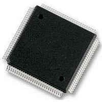
S9S12XS128J1MAL Freescale Semiconductor, S9S12XS128J1MAL Datasheet - Page 208

S9S12XS128J1MAL
Manufacturer Part Number
S9S12XS128J1MAL
Description
IC MCU 16BIT 128KB FLSH 112LQFP
Manufacturer
Freescale Semiconductor
Series
HCS12r
Datasheet
1.MC9S12XS64CAE.pdf
(738 pages)
Specifications of S9S12XS128J1MAL
Core Processor
HCS12X
Core Size
16-Bit
Speed
40MHz
Connectivity
CAN, SCI, SPI
Peripherals
LVD, POR, PWM, WDT
Number Of I /o
91
Program Memory Size
128KB (128K x 8)
Program Memory Type
FLASH
Eeprom Size
8K x 8
Ram Size
8K x 8
Voltage - Supply (vcc/vdd)
1.72 V ~ 5.5 V
Data Converters
A/D 16x12b
Oscillator Type
External
Operating Temperature
-40°C ~ 125°C
Package / Case
112-LQFP
Processor Series
S12XS
Core
HCS12
Data Bus Width
16 bit
Data Ram Size
8 KB
Interface Type
CAN, SCI, SPI
Maximum Clock Frequency
40 MHz
Number Of Programmable I/os
91
Number Of Timers
12
Maximum Operating Temperature
+ 125 C
Mounting Style
SMD/SMT
3rd Party Development Tools
EWHCS12
Development Tools By Supplier
DEMO9S12XSFAME, EVB9S12XEP100
Minimum Operating Temperature
- 40 C
On-chip Adc
12 bit, 16 Channel
Lead Free Status / RoHS Status
Lead free / RoHS Compliant
Available stocks
Company
Part Number
Manufacturer
Quantity
Price
Company:
Part Number:
S9S12XS128J1MAL
Manufacturer:
Freescale Semiconductor
Quantity:
10 000
- Current page: 208 of 738
- Download datasheet (4Mb)
S12X Debug (S12XDBGV3) Module
Comparators B and D consist of four register bytes (three address bus compare registers and a control
register).
Each set of comparator registers is accessible in the same 8-byte window of the register address map and
can be accessed using the COMRV bits in the DBGC1 register. If the Comparators B or D are accessed
through the 8-byte window, then only the address and control bytes are visible, the 4 bytes associated with
data bus and data bus masking read as zero and cannot be written. Furthermore the control registers for
comparators B and D differ from those of comparators A and C.
6.3.2.8.1
The contents of this register bits 7 and 6 differ depending upon which comparator registers are visible in
the 8-byte window of the DBG module register address map.
Read: Anytime. See
Write: If DBG not armed. See
208
Address: 0x0028
Address: 0x0028
0x002C
0x002D
0x002A
0x002B
0x002E
0x002F
0x0028
0x0029
Reset
Reset
DBGXCTL[1] is reserved. Setting this bit maps the corresponding comparator to an
W
W
R
R
SZE
0
0
0
7
7
Debug Comparator Control Register (DBGXCTL)
Figure 6-13. Debug Comparator Control Register (Comparators A and C)
Figure 6-14. Debug Comparator Control Register (Comparators B and D)
DATA HIGH COMPARATOR
DATA LOW COMPARATOR
Table 6-26
= Unimplemented or Reserved
ADDRESS MEDIUM
DATA HIGH MASK
DATA LOW MASK
ADDRESS HIGH
ADDRESS LOW
NDB
SZ
0
0
6
6
CONTROL
Table 6-26
for visible register encoding.
Table 6-25. Comparator Register Layout
S12XS Family Reference Manual, Rev. 1.11
TAG
TAG
0
0
5
5
for visible register encoding.
WARNING
BRK
BRK
0
0
4
4
Read/Write
Read/Write
Read/Write
Read/Write
Read/Write
Read/Write
Read/Write
Read/Write
RW
RW
0
0
3
3
RWE
RWE
0
0
2
2
Comparator A and C only
Comparator A and C only
Comparator A and C only
Comparator A and C only
Comparators A,B,C,D
Comparators A,B,C,D
Comparators A,B,C,D
Comparators A,B,C,D
reserved
reserved
Freescale Semiconductor
0
0
1
1
COMPE
COMPE
0
0
0
0
Related parts for S9S12XS128J1MAL
Image
Part Number
Description
Manufacturer
Datasheet
Request
R
Part Number:
Description:
Manufacturer:
Freescale Semiconductor, Inc
Datasheet:
Part Number:
Description:
Manufacturer:
Freescale Semiconductor, Inc
Datasheet:
Part Number:
Description:
Manufacturer:
Freescale Semiconductor, Inc
Datasheet:
Part Number:
Description:
Manufacturer:
Freescale Semiconductor, Inc
Datasheet:
Part Number:
Description:
Manufacturer:
Freescale Semiconductor, Inc
Datasheet:
Part Number:
Description:
Manufacturer:
Freescale Semiconductor, Inc
Datasheet:
Part Number:
Description:
Manufacturer:
Freescale Semiconductor, Inc
Datasheet:
Part Number:
Description:
Manufacturer:
Freescale Semiconductor, Inc
Datasheet:
Part Number:
Description:
Manufacturer:
Freescale Semiconductor, Inc
Datasheet:
Part Number:
Description:
Manufacturer:
Freescale Semiconductor, Inc
Datasheet:
Part Number:
Description:
Manufacturer:
Freescale Semiconductor, Inc
Datasheet:
Part Number:
Description:
Manufacturer:
Freescale Semiconductor, Inc
Datasheet:
Part Number:
Description:
Manufacturer:
Freescale Semiconductor, Inc
Datasheet:
Part Number:
Description:
Manufacturer:
Freescale Semiconductor, Inc
Datasheet:
Part Number:
Description:
Manufacturer:
Freescale Semiconductor, Inc
Datasheet:


