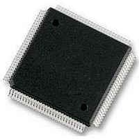
S9S12XS128J1MAL Freescale Semiconductor, S9S12XS128J1MAL Datasheet - Page 502

S9S12XS128J1MAL
Manufacturer Part Number
S9S12XS128J1MAL
Description
IC MCU 16BIT 128KB FLSH 112LQFP
Manufacturer
Freescale Semiconductor
Series
HCS12r
Datasheet
1.MC9S12XS64CAE.pdf
(738 pages)
Specifications of S9S12XS128J1MAL
Core Processor
HCS12X
Core Size
16-Bit
Speed
40MHz
Connectivity
CAN, SCI, SPI
Peripherals
LVD, POR, PWM, WDT
Number Of I /o
91
Program Memory Size
128KB (128K x 8)
Program Memory Type
FLASH
Eeprom Size
8K x 8
Ram Size
8K x 8
Voltage - Supply (vcc/vdd)
1.72 V ~ 5.5 V
Data Converters
A/D 16x12b
Oscillator Type
External
Operating Temperature
-40°C ~ 125°C
Package / Case
112-LQFP
Processor Series
S12XS
Core
HCS12
Data Bus Width
16 bit
Data Ram Size
8 KB
Interface Type
CAN, SCI, SPI
Maximum Clock Frequency
40 MHz
Number Of Programmable I/os
91
Number Of Timers
12
Maximum Operating Temperature
+ 125 C
Mounting Style
SMD/SMT
3rd Party Development Tools
EWHCS12
Development Tools By Supplier
DEMO9S12XSFAME, EVB9S12XEP100
Minimum Operating Temperature
- 40 C
On-chip Adc
12 bit, 16 Channel
Lead Free Status / RoHS Status
Lead free / RoHS Compliant
Available stocks
Company
Part Number
Manufacturer
Quantity
Price
Company:
Part Number:
S9S12XS128J1MAL
Manufacturer:
Freescale Semiconductor
Quantity:
10 000
- Current page: 502 of 738
- Download datasheet (4Mb)
Voltage Regulator (S12VREGL3V3V1)
17.4
17.4.1
Module VREG_3V3 is a voltage regulator, as depicted in
are the regulator core (REG), a low-voltage detect module (LVD), a control block (CTRL), a power-on
reset module (POR), and a low-voltage reset module (LVR)and a high temperature sensor (HTD).
17.4.2
Respectively its regulator core has three parallel, independent regulation loops (REG1,REG2 and REG3).
REG1 and REG3 differ only in the amount of current that can be delivered.
The regulators are linear regulator with a bandgap reference when operated in Full Performance Mode.
They act as a voltage clamp in Reduced Power Mode. All load currents flow from input VDDR to VSS or
VSSPLL. The reference circuits are supplied by VDDA and VSSA.
17.4.2.1
In Full Performance Mode, the output voltage is compared with a reference voltage by an operational
amplifier. The amplified input voltage difference drives the gate of an output transistor.
17.4.2.2
In Reduced Power Mode, the gate of the output transistor is connected directly to a reference voltage to
reduce power consumption. Mode switching from reduced power to full performance requires a transition
time of t
17.4.3
Subblock LVD is responsible for generating the low-voltage interrupt (LVI). LVD monitors the input
voltage (V
status flag LVDS changes its value. The LVD is available in FPM and is inactive in Reduced Power Mode
or Shutdown Mode.
17.4.4
This functional block monitors VDD. If V
the POR is deasserted. POR asserted forces the MCU into Reset. POR Deasserted will trigger the power-
on sequence.
17.4.5
Block LVR monitors the supplies VDD, VDDX and VDDF. If one (or more) drops below it’s
corresponding assertion level, signal LVR asserts; if all VDD,VDDX and VDDF supplies are above their
502
vup
Functional Description
DDA
, if the voltage regulator is enabled.
General
Regulator Core (REG)
Low-Voltage Detect (LVD)
Power-On Reset (POR)
Low-Voltage Reset (LVR)
Full Performance Mode
Reduced Power Mode
–V
SSA
) and continuously updates the status flag LVDS. Interrupt flag LVIF is set whenever
S12XS Family Reference Manual, Rev. 1.11
DD
is below V
PORD
Figure
, POR is asserted; if V
17-1. The regulator functional elements
Freescale Semiconductor
DD
exceeds V
PORD
,
Related parts for S9S12XS128J1MAL
Image
Part Number
Description
Manufacturer
Datasheet
Request
R
Part Number:
Description:
Manufacturer:
Freescale Semiconductor, Inc
Datasheet:
Part Number:
Description:
Manufacturer:
Freescale Semiconductor, Inc
Datasheet:
Part Number:
Description:
Manufacturer:
Freescale Semiconductor, Inc
Datasheet:
Part Number:
Description:
Manufacturer:
Freescale Semiconductor, Inc
Datasheet:
Part Number:
Description:
Manufacturer:
Freescale Semiconductor, Inc
Datasheet:
Part Number:
Description:
Manufacturer:
Freescale Semiconductor, Inc
Datasheet:
Part Number:
Description:
Manufacturer:
Freescale Semiconductor, Inc
Datasheet:
Part Number:
Description:
Manufacturer:
Freescale Semiconductor, Inc
Datasheet:
Part Number:
Description:
Manufacturer:
Freescale Semiconductor, Inc
Datasheet:
Part Number:
Description:
Manufacturer:
Freescale Semiconductor, Inc
Datasheet:
Part Number:
Description:
Manufacturer:
Freescale Semiconductor, Inc
Datasheet:
Part Number:
Description:
Manufacturer:
Freescale Semiconductor, Inc
Datasheet:
Part Number:
Description:
Manufacturer:
Freescale Semiconductor, Inc
Datasheet:
Part Number:
Description:
Manufacturer:
Freescale Semiconductor, Inc
Datasheet:
Part Number:
Description:
Manufacturer:
Freescale Semiconductor, Inc
Datasheet:


