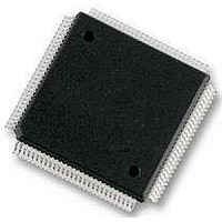
S9S12XS128J1MAL Freescale Semiconductor, S9S12XS128J1MAL Datasheet - Page 46

S9S12XS128J1MAL
Manufacturer Part Number
S9S12XS128J1MAL
Description
IC MCU 16BIT 128KB FLSH 112LQFP
Manufacturer
Freescale Semiconductor
Series
HCS12r
Datasheet
1.MC9S12XS64CAE.pdf
(738 pages)
Specifications of S9S12XS128J1MAL
Core Processor
HCS12X
Core Size
16-Bit
Speed
40MHz
Connectivity
CAN, SCI, SPI
Peripherals
LVD, POR, PWM, WDT
Number Of I /o
91
Program Memory Size
128KB (128K x 8)
Program Memory Type
FLASH
Eeprom Size
8K x 8
Ram Size
8K x 8
Voltage - Supply (vcc/vdd)
1.72 V ~ 5.5 V
Data Converters
A/D 16x12b
Oscillator Type
External
Operating Temperature
-40°C ~ 125°C
Package / Case
112-LQFP
Processor Series
S12XS
Core
HCS12
Data Bus Width
16 bit
Data Ram Size
8 KB
Interface Type
CAN, SCI, SPI
Maximum Clock Frequency
40 MHz
Number Of Programmable I/os
91
Number Of Timers
12
Maximum Operating Temperature
+ 125 C
Mounting Style
SMD/SMT
3rd Party Development Tools
EWHCS12
Development Tools By Supplier
DEMO9S12XSFAME, EVB9S12XEP100
Minimum Operating Temperature
- 40 C
On-chip Adc
12 bit, 16 Channel
Lead Free Status / RoHS Status
Lead free / RoHS Compliant
Available stocks
Company
Part Number
Manufacturer
Quantity
Price
Company:
Part Number:
S9S12XS128J1MAL
Manufacturer:
Freescale Semiconductor
Quantity:
10 000
- Current page: 46 of 738
- Download datasheet (4Mb)
Device Overview S12XS Family
1.2.4.3
The voltage supply of nominally 1.8 V is derived from the internal voltage regulator. The return current
path is through the VSS2 and VSS3 pins. No static external loading of these pins is permitted.
1.2.4.4
The voltage supply of nominally 2.8 V is derived from the internal voltage regulator. The return current
path is through the VSS1 pin. No static external loading of these pins is permitted.
1.2.4.5
These are the power supply and ground input pins for the analog-to-digital converters and the voltage
regulator.
1.2.4.6
V
1.2.4.7
These pins provide operating voltage and ground for the oscillator and the phased-locked loop. The voltage
supply of nominally 1.8 V is derived from the internal voltage regulator. This allows the supply voltage to
the oscillator and PLL to be bypassed independently. This voltage is generated by the internal voltage
regulator. No static external loading of these pins is permitted.
46
RH
and V
RL
VDD, VSS2, VSS3 — Core Power Pins
VDDF, VSS1 — NVM Power Pins
VDDA, VSSA — Power Supply Pins for ATD and Voltage Regulator
VRH, VRL — ATD Reference Voltage Input Pins
VDDPLL, VSSPLL — Power Supply Pins for PLL
are the reference voltage input pins for the analog-to-digital converter.
VSS1, VSS2,
Mnemonic
VDDX[2:1]
VSSX[2:1]
VDDR
VDDA
VSSA
VDDF
VSS3
VRH
VDD
VRL
Table 1-7. Power and Ground Connection Summary
S12XS Family Reference Manual, Rev. 1.11
Nominal
Voltage
5.0 V
5.0 V
5.0 V
5.0 V
1.8 V
2.8 V
0 V
0 V
0 V
0 V
External power supply to internal voltage
regulator
External power and ground, supply to pin
drivers
Operating voltage and ground for the
analog-to-digital converters and the
reference for the internal voltage regulator,
allows the supply voltage to the A/D to be
bypassed independently.
Reference voltages for the analog-to-digital
converter.
Internal power and ground generated by
internal regulator for the internal core.
Internal power and ground generated by
internal regulator for the internal NVM.
Description
Freescale Semiconductor
Related parts for S9S12XS128J1MAL
Image
Part Number
Description
Manufacturer
Datasheet
Request
R
Part Number:
Description:
Manufacturer:
Freescale Semiconductor, Inc
Datasheet:
Part Number:
Description:
Manufacturer:
Freescale Semiconductor, Inc
Datasheet:
Part Number:
Description:
Manufacturer:
Freescale Semiconductor, Inc
Datasheet:
Part Number:
Description:
Manufacturer:
Freescale Semiconductor, Inc
Datasheet:
Part Number:
Description:
Manufacturer:
Freescale Semiconductor, Inc
Datasheet:
Part Number:
Description:
Manufacturer:
Freescale Semiconductor, Inc
Datasheet:
Part Number:
Description:
Manufacturer:
Freescale Semiconductor, Inc
Datasheet:
Part Number:
Description:
Manufacturer:
Freescale Semiconductor, Inc
Datasheet:
Part Number:
Description:
Manufacturer:
Freescale Semiconductor, Inc
Datasheet:
Part Number:
Description:
Manufacturer:
Freescale Semiconductor, Inc
Datasheet:
Part Number:
Description:
Manufacturer:
Freescale Semiconductor, Inc
Datasheet:
Part Number:
Description:
Manufacturer:
Freescale Semiconductor, Inc
Datasheet:
Part Number:
Description:
Manufacturer:
Freescale Semiconductor, Inc
Datasheet:
Part Number:
Description:
Manufacturer:
Freescale Semiconductor, Inc
Datasheet:
Part Number:
Description:
Manufacturer:
Freescale Semiconductor, Inc
Datasheet:


