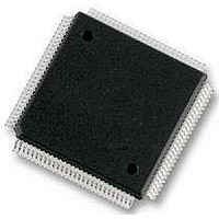
S9S12XS128J1MAL Freescale Semiconductor, S9S12XS128J1MAL Datasheet - Page 49

S9S12XS128J1MAL
Manufacturer Part Number
S9S12XS128J1MAL
Description
IC MCU 16BIT 128KB FLSH 112LQFP
Manufacturer
Freescale Semiconductor
Series
HCS12r
Datasheet
1.MC9S12XS64CAE.pdf
(738 pages)
Specifications of S9S12XS128J1MAL
Core Processor
HCS12X
Core Size
16-Bit
Speed
40MHz
Connectivity
CAN, SCI, SPI
Peripherals
LVD, POR, PWM, WDT
Number Of I /o
91
Program Memory Size
128KB (128K x 8)
Program Memory Type
FLASH
Eeprom Size
8K x 8
Ram Size
8K x 8
Voltage - Supply (vcc/vdd)
1.72 V ~ 5.5 V
Data Converters
A/D 16x12b
Oscillator Type
External
Operating Temperature
-40°C ~ 125°C
Package / Case
112-LQFP
Processor Series
S12XS
Core
HCS12
Data Bus Width
16 bit
Data Ram Size
8 KB
Interface Type
CAN, SCI, SPI
Maximum Clock Frequency
40 MHz
Number Of Programmable I/os
91
Number Of Timers
12
Maximum Operating Temperature
+ 125 C
Mounting Style
SMD/SMT
3rd Party Development Tools
EWHCS12
Development Tools By Supplier
DEMO9S12XSFAME, EVB9S12XEP100
Minimum Operating Temperature
- 40 C
On-chip Adc
12 bit, 16 Channel
Lead Free Status / RoHS Status
Lead free / RoHS Compliant
Available stocks
Company
Part Number
Manufacturer
Quantity
Price
Company:
Part Number:
S9S12XS128J1MAL
Manufacturer:
Freescale Semiconductor
Quantity:
10 000
- Current page: 49 of 738
- Download datasheet (4Mb)
The clock generated by the PLL or oscillator provides the main system clock frequencies core clock and
bus clock. As shown in
the memories, and the peripherals.
The program Flash memory is supplied by the bus clock and the oscillator clock. The oscillator clock is
used as a time base to derive the program and erase times for the NVMs.
The CAN modules may be configured to have their clock sources derived either from the bus clock or
directly from the oscillator clock. This allows the user to select its clock based on the required jitter
performance.
In order to ensure the presence of the clock the MCU includes an on-chip clock monitor connected to the
output of the oscillator. The clock monitor can be configured to invoke the PLL self-clocking mode or to
generate a system reset if it is allowed to time out as a result of no oscillator clock being present.
In addition to the clock monitor, the MCU also provides a clock quality checker which performs a more
accurate check of the clock. The clock quality checker counts a predetermined number of clock edges
within a defined time window to insure that the clock is running. The checker can be invoked following
specific events such as on wake-up or clock monitor failure.
1.4
The MCU can operate in different modes. These are described in
The MCU can operate in different power modes to facilitate power saving when full system performance
is not required. These are described in
Some modules feature a software programmable option to freeze the module status whilst the background
debug module is active to facilitate debugging. This is described in
1.4.1
The different modes and the security state of the MCU affect the debug features (enabled or disabled).
The operating mode out of reset is determined by the state of the MODC signal during reset (see
8). The MODC bit in the MODE register shows the current operating mode and provides limited mode
switching during operation. The state of the MODC signal is latched into this bit on the rising edge of
RESET.
1.4.1.1
This mode is intended for normal device operation. The opcode from the on-chip memory is being
executed after reset (requires the reset vector to be programmed correctly). The processor program is
executed from internal memory.
Freescale Semiconductor
Modes of Operation
Chip Configuration Summary
Normal Single-Chip Mode
Figure
1-6, these system clocks are used throughout the MCU to drive the core,
S12XS Family Reference Manual, Rev. 1.11
Normal single chip
Special single chip
1.4.2 Power
Chip Modes
Table 1-8. Chip Modes
Modes.
MODC
1
0
1.4.1 Chip Configuration
1.4.3 Freeze
Mode.
Device Overview S12XS Family
Summary.
Table 1-
49
Related parts for S9S12XS128J1MAL
Image
Part Number
Description
Manufacturer
Datasheet
Request
R
Part Number:
Description:
Manufacturer:
Freescale Semiconductor, Inc
Datasheet:
Part Number:
Description:
Manufacturer:
Freescale Semiconductor, Inc
Datasheet:
Part Number:
Description:
Manufacturer:
Freescale Semiconductor, Inc
Datasheet:
Part Number:
Description:
Manufacturer:
Freescale Semiconductor, Inc
Datasheet:
Part Number:
Description:
Manufacturer:
Freescale Semiconductor, Inc
Datasheet:
Part Number:
Description:
Manufacturer:
Freescale Semiconductor, Inc
Datasheet:
Part Number:
Description:
Manufacturer:
Freescale Semiconductor, Inc
Datasheet:
Part Number:
Description:
Manufacturer:
Freescale Semiconductor, Inc
Datasheet:
Part Number:
Description:
Manufacturer:
Freescale Semiconductor, Inc
Datasheet:
Part Number:
Description:
Manufacturer:
Freescale Semiconductor, Inc
Datasheet:
Part Number:
Description:
Manufacturer:
Freescale Semiconductor, Inc
Datasheet:
Part Number:
Description:
Manufacturer:
Freescale Semiconductor, Inc
Datasheet:
Part Number:
Description:
Manufacturer:
Freescale Semiconductor, Inc
Datasheet:
Part Number:
Description:
Manufacturer:
Freescale Semiconductor, Inc
Datasheet:
Part Number:
Description:
Manufacturer:
Freescale Semiconductor, Inc
Datasheet:


