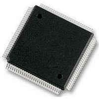
S9S12XS128J1MAL Freescale Semiconductor, S9S12XS128J1MAL Datasheet - Page 202

S9S12XS128J1MAL
Manufacturer Part Number
S9S12XS128J1MAL
Description
IC MCU 16BIT 128KB FLSH 112LQFP
Manufacturer
Freescale Semiconductor
Series
HCS12r
Datasheet
1.MC9S12XS64CAE.pdf
(738 pages)
Specifications of S9S12XS128J1MAL
Core Processor
HCS12X
Core Size
16-Bit
Speed
40MHz
Connectivity
CAN, SCI, SPI
Peripherals
LVD, POR, PWM, WDT
Number Of I /o
91
Program Memory Size
128KB (128K x 8)
Program Memory Type
FLASH
Eeprom Size
8K x 8
Ram Size
8K x 8
Voltage - Supply (vcc/vdd)
1.72 V ~ 5.5 V
Data Converters
A/D 16x12b
Oscillator Type
External
Operating Temperature
-40°C ~ 125°C
Package / Case
112-LQFP
Processor Series
S12XS
Core
HCS12
Data Bus Width
16 bit
Data Ram Size
8 KB
Interface Type
CAN, SCI, SPI
Maximum Clock Frequency
40 MHz
Number Of Programmable I/os
91
Number Of Timers
12
Maximum Operating Temperature
+ 125 C
Mounting Style
SMD/SMT
3rd Party Development Tools
EWHCS12
Development Tools By Supplier
DEMO9S12XSFAME, EVB9S12XEP100
Minimum Operating Temperature
- 40 C
On-chip Adc
12 bit, 16 Channel
Lead Free Status / RoHS Status
Lead free / RoHS Compliant
Available stocks
Company
Part Number
Manufacturer
Quantity
Price
Company:
Part Number:
S9S12XS128J1MAL
Manufacturer:
Freescale Semiconductor
Quantity:
10 000
- Current page: 202 of 738
- Download datasheet (4Mb)
S12X Debug (S12XDBGV3) Module
6.3.2.5
Read: Only when unlocked AND not secured AND not armed AND with the TSOURCE bit set.
Write: Aligned word writes when disarmed unlock the trace buffer for reading but do not affect trace buffer
contents.
202
Address: 0x0024, 0x0025
Resets
Bit[15:0]
Other
POR
Field
15–0
1
1
W
R
Currently defaults to Match2 mapped to comparator C : Match3 mapped to comparator D
Currently defaults to Match0 mapped to comparator A : Match1 mapped to comparator B
CDCM
ABCM
Bit 15 Bit 14 Bit 13 Bit 12 Bit 11 Bit 10 Bit 9
—
00
01
10
11
00
01
10
11
15
X
Trace Buffer Data Bits — The Trace Buffer Register is a window through which the 64-bit wide data lines of the
Trace Buffer may be read 16 bits at a time. Each valid read of DBGTB increments an internal trace buffer pointer
which points to the next address to be read. When the ARM bit is written to 1 the trace buffer is locked to prevent
reading. The trace buffer can only be unlocked for reading by writing to DBGTB with an aligned word write when
the module is disarmed. The DBGTB register can be read only as an aligned word, any byte reads or misaligned
access of these registers will return 0 and will not cause the trace buffer pointer to increment to the next trace
buffer address. The same is true for word reads while the debugger is armed. The POR state is undefined Other
resets do not affect the trace buffer contents. .
Debug Trace Buffer Register (DBGTBH:DBGTBL)
—
14
X
—
13
Match2 mapped to comparator C match....... Match3 mapped to comparator D match.
X
Match0 mapped to comparator A match....... Match1 mapped to comparator B match.
Figure 6-7. Debug Trace Buffer Register (DBGTB)
Match 0 mapped to comparator A/B outside range....... Match1 disabled.
Match2 mapped to comparator C/D outside range....... Match3 disabled.
—
12
Match 0 mapped to comparator A/B inside range....... Match1 disabled.
X
Match2 mapped to comparator C/D inside range....... Match3 disabled.
S12XS Family Reference Manual, Rev. 1.11
Table 6-15. DBGTB Field Descriptions
—
11
X
Table 6-13. CDCM Encoding
Table 6-14. ABCM Encoding
—
10
X
—
X
9
Bit 8
—
Description
Description
X
8
Description
Reserved
Reserved
Bit 7
—
X
7
1
1
Bit 6
—
X
6
Bit 5
—
X
5
Bit 4
—
X
4
Bit 3
—
X
3
Freescale Semiconductor
Bit 2
—
X
2
Bit 1
—
X
1
Bit 0
—
X
0
Related parts for S9S12XS128J1MAL
Image
Part Number
Description
Manufacturer
Datasheet
Request
R
Part Number:
Description:
Manufacturer:
Freescale Semiconductor, Inc
Datasheet:
Part Number:
Description:
Manufacturer:
Freescale Semiconductor, Inc
Datasheet:
Part Number:
Description:
Manufacturer:
Freescale Semiconductor, Inc
Datasheet:
Part Number:
Description:
Manufacturer:
Freescale Semiconductor, Inc
Datasheet:
Part Number:
Description:
Manufacturer:
Freescale Semiconductor, Inc
Datasheet:
Part Number:
Description:
Manufacturer:
Freescale Semiconductor, Inc
Datasheet:
Part Number:
Description:
Manufacturer:
Freescale Semiconductor, Inc
Datasheet:
Part Number:
Description:
Manufacturer:
Freescale Semiconductor, Inc
Datasheet:
Part Number:
Description:
Manufacturer:
Freescale Semiconductor, Inc
Datasheet:
Part Number:
Description:
Manufacturer:
Freescale Semiconductor, Inc
Datasheet:
Part Number:
Description:
Manufacturer:
Freescale Semiconductor, Inc
Datasheet:
Part Number:
Description:
Manufacturer:
Freescale Semiconductor, Inc
Datasheet:
Part Number:
Description:
Manufacturer:
Freescale Semiconductor, Inc
Datasheet:
Part Number:
Description:
Manufacturer:
Freescale Semiconductor, Inc
Datasheet:
Part Number:
Description:
Manufacturer:
Freescale Semiconductor, Inc
Datasheet:


