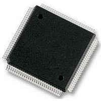
S9S12XS128J1MAL Freescale Semiconductor, S9S12XS128J1MAL Datasheet - Page 441

S9S12XS128J1MAL
Manufacturer Part Number
S9S12XS128J1MAL
Description
IC MCU 16BIT 128KB FLSH 112LQFP
Manufacturer
Freescale Semiconductor
Series
HCS12r
Datasheet
1.MC9S12XS64CAE.pdf
(738 pages)
Specifications of S9S12XS128J1MAL
Core Processor
HCS12X
Core Size
16-Bit
Speed
40MHz
Connectivity
CAN, SCI, SPI
Peripherals
LVD, POR, PWM, WDT
Number Of I /o
91
Program Memory Size
128KB (128K x 8)
Program Memory Type
FLASH
Eeprom Size
8K x 8
Ram Size
8K x 8
Voltage - Supply (vcc/vdd)
1.72 V ~ 5.5 V
Data Converters
A/D 16x12b
Oscillator Type
External
Operating Temperature
-40°C ~ 125°C
Package / Case
112-LQFP
Processor Series
S12XS
Core
HCS12
Data Bus Width
16 bit
Data Ram Size
8 KB
Interface Type
CAN, SCI, SPI
Maximum Clock Frequency
40 MHz
Number Of Programmable I/os
91
Number Of Timers
12
Maximum Operating Temperature
+ 125 C
Mounting Style
SMD/SMT
3rd Party Development Tools
EWHCS12
Development Tools By Supplier
DEMO9S12XSFAME, EVB9S12XEP100
Minimum Operating Temperature
- 40 C
On-chip Adc
12 bit, 16 Channel
Lead Free Status / RoHS Status
Lead free / RoHS Compliant
Available stocks
Company
Part Number
Manufacturer
Quantity
Price
Company:
Part Number:
S9S12XS128J1MAL
Manufacturer:
Freescale Semiconductor
Quantity:
10 000
- Current page: 441 of 738
- Download datasheet (4Mb)
1
Freescale Semiconductor
MODFEN
n is used later in this document as a placeholder for the selected transfer width.
BIDIROE
SPISWAI
XFRW
SPC0
Field
6
4
3
1
0
Transfer Width — This bit is used for selecting the data transfer width. If 8-bit transfer width is selected, SPIDRL
becomes the dedicated data register and SPIDRH is unused. If 16-bit transfer width is selected, SPIDRH and
SPIDRL form a 16-bit data register. Please refer to
information about transmit/receive data handling and the interrupt flag clearing mechanism. In master mode, a
change of this bit will abort a transmission in progress and force the SPI system into idle state.
0 8-bit Transfer Width (n = 8)
1 16-bit Transfer Width (n = 16)
Mode Fault Enable Bit — This bit allows the MODF failure to be detected. If the SPI is in master mode and
MODFEN is cleared, then the SS port pin is not used by the SPI. In slave mode, the SS is available only as an
input regardless of the value of MODFEN. For an overview on the impact of the MODFEN bit on the SS port pin
configuration, refer to
force the SPI system into idle state.
0 SS port pin is not used by the SPI.
1 SS port pin with MODF feature.
Output Enable in the Bidirectional Mode of Operation — This bit controls the MOSI and MISO output buffer
of the SPI, when in bidirectional mode of operation (SPC0 is set). In master mode, this bit controls the output
buffer of the MOSI port, in slave mode it controls the output buffer of the MISO port. In master mode, with SPC0
set, a change of this bit will abort a transmission in progress and force the SPI into idle state.
0 Output buffer disabled.
1 Output buffer enabled.
SPI Stop in Wait Mode Bit — This bit is used for power conservation while in wait mode.
0 SPI clock operates normally in wait mode.
1 Stop SPI clock generation when in wait mode.
Serial Pin Control Bit 0 — This bit enables bidirectional pin configurations as shown in
mode, a change of this bit will abort a transmission in progress and force the SPI system into idle state.
Bidirectional
Bidirectional
Pin Mode
Normal
Normal
SPC0
0
1
0
1
Table
Table 15-5. Bidirectional Pin Configurations
S12XS Family Reference Manual, Rev. 1.11
Table 15-4. SPICR2 Field Descriptions
BIDIROE
15-3. In master mode, a change of this bit will abort a transmission in progress and
1
X
X
0
1
0
1
1
Master Mode of Operation
Slave Mode of Operation
MISO not used by SPI
Slave Out
Master In
Slave I/O
Description
Slave In
MISO
Section 15.3.2.4, “SPI Status Register (SPISR)
MOSI not used by SPI
Serial Peripheral Interface (S12SPIV5)
Master Out
Master I/O
Master In
Slave In
MOSI
Table
15-5. In master
for
441
Related parts for S9S12XS128J1MAL
Image
Part Number
Description
Manufacturer
Datasheet
Request
R
Part Number:
Description:
Manufacturer:
Freescale Semiconductor, Inc
Datasheet:
Part Number:
Description:
Manufacturer:
Freescale Semiconductor, Inc
Datasheet:
Part Number:
Description:
Manufacturer:
Freescale Semiconductor, Inc
Datasheet:
Part Number:
Description:
Manufacturer:
Freescale Semiconductor, Inc
Datasheet:
Part Number:
Description:
Manufacturer:
Freescale Semiconductor, Inc
Datasheet:
Part Number:
Description:
Manufacturer:
Freescale Semiconductor, Inc
Datasheet:
Part Number:
Description:
Manufacturer:
Freescale Semiconductor, Inc
Datasheet:
Part Number:
Description:
Manufacturer:
Freescale Semiconductor, Inc
Datasheet:
Part Number:
Description:
Manufacturer:
Freescale Semiconductor, Inc
Datasheet:
Part Number:
Description:
Manufacturer:
Freescale Semiconductor, Inc
Datasheet:
Part Number:
Description:
Manufacturer:
Freescale Semiconductor, Inc
Datasheet:
Part Number:
Description:
Manufacturer:
Freescale Semiconductor, Inc
Datasheet:
Part Number:
Description:
Manufacturer:
Freescale Semiconductor, Inc
Datasheet:
Part Number:
Description:
Manufacturer:
Freescale Semiconductor, Inc
Datasheet:
Part Number:
Description:
Manufacturer:
Freescale Semiconductor, Inc
Datasheet:


