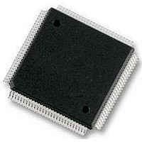
S9S12XS128J1MAL Freescale Semiconductor, S9S12XS128J1MAL Datasheet - Page 277

S9S12XS128J1MAL
Manufacturer Part Number
S9S12XS128J1MAL
Description
IC MCU 16BIT 128KB FLSH 112LQFP
Manufacturer
Freescale Semiconductor
Series
HCS12r
Datasheet
1.MC9S12XS64CAE.pdf
(738 pages)
Specifications of S9S12XS128J1MAL
Core Processor
HCS12X
Core Size
16-Bit
Speed
40MHz
Connectivity
CAN, SCI, SPI
Peripherals
LVD, POR, PWM, WDT
Number Of I /o
91
Program Memory Size
128KB (128K x 8)
Program Memory Type
FLASH
Eeprom Size
8K x 8
Ram Size
8K x 8
Voltage - Supply (vcc/vdd)
1.72 V ~ 5.5 V
Data Converters
A/D 16x12b
Oscillator Type
External
Operating Temperature
-40°C ~ 125°C
Package / Case
112-LQFP
Processor Series
S12XS
Core
HCS12
Data Bus Width
16 bit
Data Ram Size
8 KB
Interface Type
CAN, SCI, SPI
Maximum Clock Frequency
40 MHz
Number Of Programmable I/os
91
Number Of Timers
12
Maximum Operating Temperature
+ 125 C
Mounting Style
SMD/SMT
3rd Party Development Tools
EWHCS12
Development Tools By Supplier
DEMO9S12XSFAME, EVB9S12XEP100
Minimum Operating Temperature
- 40 C
On-chip Adc
12 bit, 16 Channel
Lead Free Status / RoHS Status
Lead free / RoHS Compliant
Available stocks
Company
Part Number
Manufacturer
Quantity
Price
Company:
Part Number:
S9S12XS128J1MAL
Manufacturer:
Freescale Semiconductor
Quantity:
10 000
- Current page: 277 of 738
- Download datasheet (4Mb)
10.3.2.2
Writes to this register will abort current conversion sequence.
Read: Anytime
Write: Anytime
Freescale Semiconductor
ETRIGCH[3:0]
Module Base + 0x0001
ETRIGSEL
SRES[1:0]
SMP_DIS
Reset
Field
6–5
3–0
W
7
4
R
ETRIGSEL
ATD Control Register 1 (ATDCTL1)
0
7
External Trigger Source Select — This bit selects the external trigger source to be either one of the AD
channels or one of the ETRIG3-0 inputs. See device specification for availability and connectivity of ETRIG3-
0 inputs. If a particular ETRIG3-0 input option is not available, writing a 1 to ETRISEL only sets the bit but has
not effect, this means that one of the AD channels (selected by ETRIGCH3-0) is configured as the source for
external trigger. The coding is summarized in
A/D Resolution Select — These bits select the resolution of A/D conversion results. See
coding.
Discharge Before Sampling Bit
0 No discharge before sampling.
1 The internal sample capacitor is discharged before sampling the channel. This adds 2 ATD clock cycles to
External Trigger Channel Select — These bits select one of the AD channels or one of the ETRIG3-0 inputs
as source for the external trigger. The coding is summarized in
1
the sampling time. This can help to detect an open circuit instead of measuring the previous sampled
channel.
If only AN0 should be converted use MULT=0.
SRES1
0
6
SRES1
Figure 10-4. ATD Control Register 1 (ATDCTL1)
0
0
1
1
Table 10-3. ATDCTL1 Field Descriptions
S12XS Family Reference Manual, Rev. 1.11
SRES0
Table 10-4. A/D Resolution Coding
1
5
SRES0
0
1
0
1
SMP_DIS
0
4
Table
Description
10-5.
ETRIGCH3
A/D Resolution
10-bit data
12-bit data
Reserved
1
8-bit data
3
Table
Analog-to-Digital Converter (ADC12B16CV1)
ETRIGCH2
10-5.
1
2
ETRIGCH1
1
1
Table 10-4
ETRIGCH0
for
1
0
277
Related parts for S9S12XS128J1MAL
Image
Part Number
Description
Manufacturer
Datasheet
Request
R
Part Number:
Description:
Manufacturer:
Freescale Semiconductor, Inc
Datasheet:
Part Number:
Description:
Manufacturer:
Freescale Semiconductor, Inc
Datasheet:
Part Number:
Description:
Manufacturer:
Freescale Semiconductor, Inc
Datasheet:
Part Number:
Description:
Manufacturer:
Freescale Semiconductor, Inc
Datasheet:
Part Number:
Description:
Manufacturer:
Freescale Semiconductor, Inc
Datasheet:
Part Number:
Description:
Manufacturer:
Freescale Semiconductor, Inc
Datasheet:
Part Number:
Description:
Manufacturer:
Freescale Semiconductor, Inc
Datasheet:
Part Number:
Description:
Manufacturer:
Freescale Semiconductor, Inc
Datasheet:
Part Number:
Description:
Manufacturer:
Freescale Semiconductor, Inc
Datasheet:
Part Number:
Description:
Manufacturer:
Freescale Semiconductor, Inc
Datasheet:
Part Number:
Description:
Manufacturer:
Freescale Semiconductor, Inc
Datasheet:
Part Number:
Description:
Manufacturer:
Freescale Semiconductor, Inc
Datasheet:
Part Number:
Description:
Manufacturer:
Freescale Semiconductor, Inc
Datasheet:
Part Number:
Description:
Manufacturer:
Freescale Semiconductor, Inc
Datasheet:
Part Number:
Description:
Manufacturer:
Freescale Semiconductor, Inc
Datasheet:


