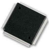
S9S12XS128J1MAL Freescale Semiconductor, S9S12XS128J1MAL Datasheet - Page 543

S9S12XS128J1MAL
Manufacturer Part Number
S9S12XS128J1MAL
Description
IC MCU 16BIT 128KB FLSH 112LQFP
Manufacturer
Freescale Semiconductor
Series
HCS12r
Datasheet
1.MC9S12XS64CAE.pdf
(738 pages)
Specifications of S9S12XS128J1MAL
Core Processor
HCS12X
Core Size
16-Bit
Speed
40MHz
Connectivity
CAN, SCI, SPI
Peripherals
LVD, POR, PWM, WDT
Number Of I /o
91
Program Memory Size
128KB (128K x 8)
Program Memory Type
FLASH
Eeprom Size
8K x 8
Ram Size
8K x 8
Voltage - Supply (vcc/vdd)
1.72 V ~ 5.5 V
Data Converters
A/D 16x12b
Oscillator Type
External
Operating Temperature
-40°C ~ 125°C
Package / Case
112-LQFP
Processor Series
S12XS
Core
HCS12
Data Bus Width
16 bit
Data Ram Size
8 KB
Interface Type
CAN, SCI, SPI
Maximum Clock Frequency
40 MHz
Number Of Programmable I/os
91
Number Of Timers
12
Maximum Operating Temperature
+ 125 C
Mounting Style
SMD/SMT
3rd Party Development Tools
EWHCS12
Development Tools By Supplier
DEMO9S12XSFAME, EVB9S12XEP100
Minimum Operating Temperature
- 40 C
On-chip Adc
12 bit, 16 Channel
Lead Free Status / RoHS Status
Lead free / RoHS Compliant
Available stocks
Company
Part Number
Manufacturer
Quantity
Price
Company:
Part Number:
S9S12XS128J1MAL
Manufacturer:
Freescale Semiconductor
Quantity:
10 000
- Current page: 543 of 738
- Download datasheet (4Mb)
phrase index values for the Read Once command range from 0x0000 to 0x0007. During execution of the
Read Once command, any attempt to read addresses within P-Flash block will return invalid data.
18.4.2.5
The Program P-Flash operation will program a previously erased phrase in the P-Flash memory using an
embedded algorithm.
Upon clearing CCIF to launch the Program P-Flash command, the Memory Controller will program the
data words to the supplied global address and will then proceed to verify the data words read back as
expected. The CCIF flag will set after the Program P-Flash operation has completed.
Freescale Semiconductor
Register
FSTAT
Program P-Flash Command
A P-Flash phrase must be in the erased state before being programmed.
Cumulative programming of bits within a Flash phrase is not allowed.
1
CCOBIX[2:0]
Table 18-39. Program P-Flash Command FCCOB Requirements
Global address [2:0] must be 000
MGSTAT1
MGSTAT0
ACCERR
Error Bit
FPVIOL
000
001
010
011
100
101
Table 18-38. Read Once Command Error Handling
S12XS Family Reference Manual, Rev. 1.11
Set if CCOBIX[2:0] != 001 at command launch
Set if command not available in current mode (see
Set if an invalid phrase index is supplied
None
Set if any errors have been encountered during the read
Set if any non-correctable errors have been encountered during the read
Global address [15:0] of phrase location to be programmed
0x06
CAUTION
Word 0 program value
Word 1 program value
Word 2 program value
Word 3 program value
FCCOB Parameters
Error Condition
Global address [22:16] to
identify P-Flash block
256 KByte Flash Module (S12XFTMR256K1V1)
Table
18-28)
1
543
Related parts for S9S12XS128J1MAL
Image
Part Number
Description
Manufacturer
Datasheet
Request
R
Part Number:
Description:
Manufacturer:
Freescale Semiconductor, Inc
Datasheet:
Part Number:
Description:
Manufacturer:
Freescale Semiconductor, Inc
Datasheet:
Part Number:
Description:
Manufacturer:
Freescale Semiconductor, Inc
Datasheet:
Part Number:
Description:
Manufacturer:
Freescale Semiconductor, Inc
Datasheet:
Part Number:
Description:
Manufacturer:
Freescale Semiconductor, Inc
Datasheet:
Part Number:
Description:
Manufacturer:
Freescale Semiconductor, Inc
Datasheet:
Part Number:
Description:
Manufacturer:
Freescale Semiconductor, Inc
Datasheet:
Part Number:
Description:
Manufacturer:
Freescale Semiconductor, Inc
Datasheet:
Part Number:
Description:
Manufacturer:
Freescale Semiconductor, Inc
Datasheet:
Part Number:
Description:
Manufacturer:
Freescale Semiconductor, Inc
Datasheet:
Part Number:
Description:
Manufacturer:
Freescale Semiconductor, Inc
Datasheet:
Part Number:
Description:
Manufacturer:
Freescale Semiconductor, Inc
Datasheet:
Part Number:
Description:
Manufacturer:
Freescale Semiconductor, Inc
Datasheet:
Part Number:
Description:
Manufacturer:
Freescale Semiconductor, Inc
Datasheet:
Part Number:
Description:
Manufacturer:
Freescale Semiconductor, Inc
Datasheet:


