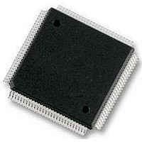
S9S12XS128J1MAL Freescale Semiconductor, S9S12XS128J1MAL Datasheet - Page 283

S9S12XS128J1MAL
Manufacturer Part Number
S9S12XS128J1MAL
Description
IC MCU 16BIT 128KB FLSH 112LQFP
Manufacturer
Freescale Semiconductor
Series
HCS12r
Datasheet
1.MC9S12XS64CAE.pdf
(738 pages)
Specifications of S9S12XS128J1MAL
Core Processor
HCS12X
Core Size
16-Bit
Speed
40MHz
Connectivity
CAN, SCI, SPI
Peripherals
LVD, POR, PWM, WDT
Number Of I /o
91
Program Memory Size
128KB (128K x 8)
Program Memory Type
FLASH
Eeprom Size
8K x 8
Ram Size
8K x 8
Voltage - Supply (vcc/vdd)
1.72 V ~ 5.5 V
Data Converters
A/D 16x12b
Oscillator Type
External
Operating Temperature
-40°C ~ 125°C
Package / Case
112-LQFP
Processor Series
S12XS
Core
HCS12
Data Bus Width
16 bit
Data Ram Size
8 KB
Interface Type
CAN, SCI, SPI
Maximum Clock Frequency
40 MHz
Number Of Programmable I/os
91
Number Of Timers
12
Maximum Operating Temperature
+ 125 C
Mounting Style
SMD/SMT
3rd Party Development Tools
EWHCS12
Development Tools By Supplier
DEMO9S12XSFAME, EVB9S12XEP100
Minimum Operating Temperature
- 40 C
On-chip Adc
12 bit, 16 Channel
Lead Free Status / RoHS Status
Lead free / RoHS Compliant
Available stocks
Company
Part Number
Manufacturer
Quantity
Price
Company:
Part Number:
S9S12XS128J1MAL
Manufacturer:
Freescale Semiconductor
Quantity:
10 000
- Current page: 283 of 738
- Download datasheet (4Mb)
10.3.2.6
Writes to this register will abort current conversion sequence and start a new conversion sequence. If
external trigger is enabled (ETRIGE=1) an initial write to ATDCTL5 is required to allow starting of a
conversion sequence which will then occur on each trigger event. Start of conversion means the beginning
of the sampling phase.
Read: Anytime
Write: Anytime
Freescale Semiconductor
Module Base + 0x0005
Reset
SCAN
Field
SC
6
5
W
R
Special Channel Conversion Bit — If this bit is set, then special channel conversion can be selected using CD,
CC, CB and CA of ATDCTL5.
0 Special channel conversions disabled
1 Special channel conversions enabled
Continuous Conversion Sequence Mode — This bit selects whether conversion sequences are performed
continuously or only once. If external trigger is enabled (ETRIGE=1) setting this bit has no effect, that means
external trigger always starts a single conversion sequence.
0 Single conversion sequence
1 Continuous conversion sequences (scan mode)
ATD Control Register 5 (ATDCTL5)
0
0
7
SMP2
SC
0
6
1
Figure 10-8. ATD Control Register 5 (ATDCTL5)
Table 10-14. ATDCTL5 Field Descriptions
S12XS Family Reference Manual, Rev. 1.11
SMP1
SCAN
Table 10-13. Sample Time Select
Table 10-15
1
0
5
SMP0
lists the coding.
MULT
1
0
4
Description
ATD Clock Cycles
CD
0
3
Sample Time
in Number of
24
Analog-to-Digital Converter (ADC12B16CV1)
CC
0
2
CB
0
1
CA
0
0
283
Related parts for S9S12XS128J1MAL
Image
Part Number
Description
Manufacturer
Datasheet
Request
R
Part Number:
Description:
Manufacturer:
Freescale Semiconductor, Inc
Datasheet:
Part Number:
Description:
Manufacturer:
Freescale Semiconductor, Inc
Datasheet:
Part Number:
Description:
Manufacturer:
Freescale Semiconductor, Inc
Datasheet:
Part Number:
Description:
Manufacturer:
Freescale Semiconductor, Inc
Datasheet:
Part Number:
Description:
Manufacturer:
Freescale Semiconductor, Inc
Datasheet:
Part Number:
Description:
Manufacturer:
Freescale Semiconductor, Inc
Datasheet:
Part Number:
Description:
Manufacturer:
Freescale Semiconductor, Inc
Datasheet:
Part Number:
Description:
Manufacturer:
Freescale Semiconductor, Inc
Datasheet:
Part Number:
Description:
Manufacturer:
Freescale Semiconductor, Inc
Datasheet:
Part Number:
Description:
Manufacturer:
Freescale Semiconductor, Inc
Datasheet:
Part Number:
Description:
Manufacturer:
Freescale Semiconductor, Inc
Datasheet:
Part Number:
Description:
Manufacturer:
Freescale Semiconductor, Inc
Datasheet:
Part Number:
Description:
Manufacturer:
Freescale Semiconductor, Inc
Datasheet:
Part Number:
Description:
Manufacturer:
Freescale Semiconductor, Inc
Datasheet:
Part Number:
Description:
Manufacturer:
Freescale Semiconductor, Inc
Datasheet:


