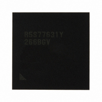
R5S77631Y266BGV Renesas Electronics America, R5S77631Y266BGV Datasheet - Page 50

R5S77631Y266BGV
Manufacturer Part Number
R5S77631Y266BGV
Description
IC SUPERH MPU ROMLESS 499BGA
Manufacturer
Renesas Electronics America
Series
SuperH® SH7780r
Datasheet
1.R5S77631Y266BGV.pdf
(2056 pages)
Specifications of R5S77631Y266BGV
Core Processor
SH-4A
Core Size
32-Bit
Speed
266MHz
Connectivity
Audio Codec, I²C, MMC, SCI, SIM, SIO, SSI, USB
Peripherals
DMA, LCD, POR, WDT
Number Of I /o
107
Program Memory Type
ROMless
Ram Size
16K x 8
Voltage - Supply (vcc/vdd)
1.15 V ~ 1.35 V
Data Converters
A/D 4x10b; D/A 2x8b
Oscillator Type
External
Operating Temperature
-20°C ~ 75°C
Package / Case
499-BGA
Lead Free Status / RoHS Status
Lead free / RoHS Compliant
Eeprom Size
-
Program Memory Size
-
Available stocks
Company
Part Number
Manufacturer
Quantity
Price
Company:
Part Number:
R5S77631Y266BGV
Manufacturer:
Renesas Electronics America
Quantity:
10 000
- Current page: 50 of 2056
- Download datasheet (10Mb)
Figure 27.13 Sample SCIF Receive Operation
Figure 27.14 Sample Operation Using Modem Control (SCIF0_RTS)
Figure 27.15 Data Format in Clocked Synchronous Communication ...................................... 1106
Figure 27.16 Sample SCIF Initialization Flowchart ................................................................. 1108
Figure 27.17 Sample Serial Transmission Flowchart ............................................................... 1109
Figure 27.18 Sample SCIF Transmission Operation in Clocked Synchronous Mode.............. 1110
Figure 27.19 Sample Serial Reception Flowchart (1)............................................................... 1111
Figure 27.19 Sample Serial Reception Flowchart (2)............................................................... 1112
Figure 27.20 Sample SCIF Reception Operation in Clocked Synchronous Mode ................... 1113
Figure 27.21 Sample Simultaneous Serial Transmission and Reception Flowchart................. 1114
Figure 27.22 Receive Data Sampling Timing in Asynchronous Mode .................................... 1118
Figure 27.23 Example of Synchronization Clock Transfer by DMAC .................................... 1119
Section 28 Serial Communication Interface with FIFO/IrDA Interface (SCIF/IrDA)
Figure 28.1 Block Diagram of SCIF/IrDA ............................................................................... 1123
Figure 28.2 SCIF2_SCK Pin .................................................................................................... 1124
Figure 28.3 SCIF2_TXD Pin.................................................................................................... 1124
Figure 28.4 SCIF2_RXD Pin.................................................................................................... 1125
Figure 28.5 Data Format in Asynchronous Communication
Figure 28.6 Sample SCIF Initialization Flowchart ................................................................... 1160
Figure 28.7 Sample Serial Transmission Flowchart ................................................................. 1161
Figure 28.8 Sample SCIF Transmission Operation
Figure 28.9 Sample Serial Reception Flowchart (1)................................................................. 1164
Figure 28.10 Sample Serial Reception Flowchart (2)............................................................... 1165
Figure 28.11 Sample SCIF Receive Operation
Figure 28.12 Data Format in Clocked Synchronous Communication ...................................... 1167
Figure 28.13 Sample SCIF Initialization Flowchart ................................................................. 1169
Figure 28.14 Sample Serial Transmission Flowchart ............................................................... 1170
Figure 28.15 Sample SCIF Transmission Operation in Clocked Synchronous Mode.............. 1171
Figure 28.16 Sample Serial Reception Flowchart (1)............................................................... 1172
Figure 28.17 Sample Serial Reception Flowchart (2)............................................................... 1173
Figure 28.18 Sample SCIF Reception Operation in Clocked Synchronous Mode ................... 1174
Figure 28.19 Sample Simultaneous Serial Transmission and Reception Flowchart................. 1175
Figure 28.20 Receive Data Sampling Timing in Asynchronous Mode .................................... 1179
Figure 28.21 Infrared Communication Data Format ................................................................ 1181
Figure 28.22 Block Diagram of Infrared Data Communication Interface ................................ 1182
Rev. 2.00 May 22, 2009 Page xlviii of lxviii
(Example with 8-Bit Data, Parity, and Two Stop Bits) ......................................... 1157
(Example with 8-Bit Data, Parity, One Stop Bit) .................................................. 1163
(Example with 8-Bit Data, Parity, One Stop Bit) ................................................ 1105
(Only in Channel 0) ............................................................................................. 1106
(Example with 8-Bit Data, Parity, One Stop Bit) ................................................ 1167
Related parts for R5S77631Y266BGV
Image
Part Number
Description
Manufacturer
Datasheet
Request
R

Part Number:
Description:
KIT STARTER FOR M16C/29
Manufacturer:
Renesas Electronics America
Datasheet:

Part Number:
Description:
KIT STARTER FOR R8C/2D
Manufacturer:
Renesas Electronics America
Datasheet:

Part Number:
Description:
R0K33062P STARTER KIT
Manufacturer:
Renesas Electronics America
Datasheet:

Part Number:
Description:
KIT STARTER FOR R8C/23 E8A
Manufacturer:
Renesas Electronics America
Datasheet:

Part Number:
Description:
KIT STARTER FOR R8C/25
Manufacturer:
Renesas Electronics America
Datasheet:

Part Number:
Description:
KIT STARTER H8S2456 SHARPE DSPLY
Manufacturer:
Renesas Electronics America
Datasheet:

Part Number:
Description:
KIT STARTER FOR R8C38C
Manufacturer:
Renesas Electronics America
Datasheet:

Part Number:
Description:
KIT STARTER FOR R8C35C
Manufacturer:
Renesas Electronics America
Datasheet:

Part Number:
Description:
KIT STARTER FOR R8CL3AC+LCD APPS
Manufacturer:
Renesas Electronics America
Datasheet:

Part Number:
Description:
KIT STARTER FOR RX610
Manufacturer:
Renesas Electronics America
Datasheet:

Part Number:
Description:
KIT STARTER FOR R32C/118
Manufacturer:
Renesas Electronics America
Datasheet:

Part Number:
Description:
KIT DEV RSK-R8C/26-29
Manufacturer:
Renesas Electronics America
Datasheet:

Part Number:
Description:
KIT STARTER FOR SH7124
Manufacturer:
Renesas Electronics America
Datasheet:

Part Number:
Description:
KIT STARTER FOR H8SX/1622
Manufacturer:
Renesas Electronics America
Datasheet:

Part Number:
Description:
KIT DEV FOR SH7203
Manufacturer:
Renesas Electronics America
Datasheet:


