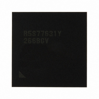
R5S77631Y266BGV Renesas Electronics America, R5S77631Y266BGV Datasheet - Page 269

R5S77631Y266BGV
Manufacturer Part Number
R5S77631Y266BGV
Description
IC SUPERH MPU ROMLESS 499BGA
Manufacturer
Renesas Electronics America
Series
SuperH® SH7780r
Datasheet
1.R5S77631Y266BGV.pdf
(2056 pages)
Specifications of R5S77631Y266BGV
Core Processor
SH-4A
Core Size
32-Bit
Speed
266MHz
Connectivity
Audio Codec, I²C, MMC, SCI, SIM, SIO, SSI, USB
Peripherals
DMA, LCD, POR, WDT
Number Of I /o
107
Program Memory Type
ROMless
Ram Size
16K x 8
Voltage - Supply (vcc/vdd)
1.15 V ~ 1.35 V
Data Converters
A/D 4x10b; D/A 2x8b
Oscillator Type
External
Operating Temperature
-20°C ~ 75°C
Package / Case
499-BGA
Lead Free Status / RoHS Status
Lead free / RoHS Compliant
Eeprom Size
-
Program Memory Size
-
Available stocks
Company
Part Number
Manufacturer
Quantity
Price
Company:
Part Number:
R5S77631Y266BGV
Manufacturer:
Renesas Electronics America
Quantity:
10 000
- Current page: 269 of 2056
- Download datasheet (10Mb)
5. Cache miss (with write-back)
7.3.3
When the Operand cache (OC) is enabled (OCE = 1 in CCR) and data is written to a cacheable
area, the cache operates as follows:
1. The tag, V bit, U bit, and LRU bits on each way are read from the cache line indexed by virtual
2. The tag, read from each way, is compared with bits [28:10] of the physical address resulting
• If there is a way whose tag matches and its V bit is 1, see No. 3 for copy-back and No. 4 for
• I If there is no way whose tag matches and its V bit is 1 and the U bit of the way which is
• If there is no way whose tag matches and its V bit is 1 and the U bit of the way which is
3. Cache hit (copy-back)
4. Cache hit (write-through)
The tag and data field of the cache line on the way which is selected to replace are saved in the
write-back buffer. Then data is read into the cache line on the way which is selected to replace
from the physical address space corresponding to the virtual address. Data reading is
performed, using the wraparound method, in order from the quad-word data (8 bytes)
including the cache-missed data. In the prefetch operation the CPU doesn't wait the data
arrives. While the one cache line of data is being read, the CPU can execute the next
processing. And the LRU bits are updated to indicate the way is latest one. The data in the
write-back buffer is then written back to external memory.
address bits [12:5].
from virtual address translation by the MMU:
write-through.
selected to replace using the LRU bits is 0, see No. 5 for copy-back and No. 7 for write-
through.
selected to replace using the LRU bits is 1, see No. 6 for copy-back and No. 7 for write-
through.
A data write in accordance with the access size is performed for the data field on the hit way
which is indexed by virtual address bits [4:0]. Then 1 is written to the U bit. The LRU bits are
updated to indicate the way is the latest one.
A data write in accordance with the access size is performed for the data field on the hit way
which is indexed by virtual address bits [4:0]. A write is also performed to external memory
corresponding to the virtual address. Then the LRU bits are updated to indicate the way is the
latest one. In this case, the U bit isn't updated.
Write Operation
Rev. 2.00 May 22, 2009 Page 199 of 1982
Section 7 Caches
REJ09B0256-0200
Related parts for R5S77631Y266BGV
Image
Part Number
Description
Manufacturer
Datasheet
Request
R

Part Number:
Description:
KIT STARTER FOR M16C/29
Manufacturer:
Renesas Electronics America
Datasheet:

Part Number:
Description:
KIT STARTER FOR R8C/2D
Manufacturer:
Renesas Electronics America
Datasheet:

Part Number:
Description:
R0K33062P STARTER KIT
Manufacturer:
Renesas Electronics America
Datasheet:

Part Number:
Description:
KIT STARTER FOR R8C/23 E8A
Manufacturer:
Renesas Electronics America
Datasheet:

Part Number:
Description:
KIT STARTER FOR R8C/25
Manufacturer:
Renesas Electronics America
Datasheet:

Part Number:
Description:
KIT STARTER H8S2456 SHARPE DSPLY
Manufacturer:
Renesas Electronics America
Datasheet:

Part Number:
Description:
KIT STARTER FOR R8C38C
Manufacturer:
Renesas Electronics America
Datasheet:

Part Number:
Description:
KIT STARTER FOR R8C35C
Manufacturer:
Renesas Electronics America
Datasheet:

Part Number:
Description:
KIT STARTER FOR R8CL3AC+LCD APPS
Manufacturer:
Renesas Electronics America
Datasheet:

Part Number:
Description:
KIT STARTER FOR RX610
Manufacturer:
Renesas Electronics America
Datasheet:

Part Number:
Description:
KIT STARTER FOR R32C/118
Manufacturer:
Renesas Electronics America
Datasheet:

Part Number:
Description:
KIT DEV RSK-R8C/26-29
Manufacturer:
Renesas Electronics America
Datasheet:

Part Number:
Description:
KIT STARTER FOR SH7124
Manufacturer:
Renesas Electronics America
Datasheet:

Part Number:
Description:
KIT STARTER FOR H8SX/1622
Manufacturer:
Renesas Electronics America
Datasheet:

Part Number:
Description:
KIT DEV FOR SH7203
Manufacturer:
Renesas Electronics America
Datasheet:


