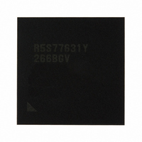
R5S77631Y266BGV Renesas Electronics America, R5S77631Y266BGV Datasheet - Page 254

R5S77631Y266BGV
Manufacturer Part Number
R5S77631Y266BGV
Description
IC SUPERH MPU ROMLESS 499BGA
Manufacturer
Renesas Electronics America
Series
SuperH® SH7780r
Datasheet
1.R5S77631Y266BGV.pdf
(2056 pages)
Specifications of R5S77631Y266BGV
Core Processor
SH-4A
Core Size
32-Bit
Speed
266MHz
Connectivity
Audio Codec, I²C, MMC, SCI, SIM, SIO, SSI, USB
Peripherals
DMA, LCD, POR, WDT
Number Of I /o
107
Program Memory Type
ROMless
Ram Size
16K x 8
Voltage - Supply (vcc/vdd)
1.15 V ~ 1.35 V
Data Converters
A/D 4x10b; D/A 2x8b
Oscillator Type
External
Operating Temperature
-20°C ~ 75°C
Package / Case
499-BGA
Lead Free Status / RoHS Status
Lead free / RoHS Compliant
Eeprom Size
-
Program Memory Size
-
Available stocks
Company
Part Number
Manufacturer
Quantity
Price
Company:
Part Number:
R5S77631Y266BGV
Manufacturer:
Renesas Electronics America
Quantity:
10 000
- Current page: 254 of 2056
- Download datasheet (10Mb)
Section 6 Memory Management Unit (MMU)
6.7.6
When using 32-bit address extended mode, note that the items described in this section are
extended or changed as follows.
PASCR: The SE bit is added in bit 31 in the control register (PASCR). The bits 6 to 0 of the UB
in the PASCR are invalid (Note that the bit 7 of the UB is still valid). When writing to the P1 or
P2 area, the UB bit in the PMB controls whether a buffered write is performed or not. When the
MMU is enabled, the UB bit in the TLB controls writing to the P0, P3, or U0 area. When the
MMU is disabled, writing to the P0, P3, or U0 area is always performed as a buffered write.
ITLB: The PPN field in the ITLB is extended to bits 31 to 10.
UTLB: The PPN field in the UTLB is extended to bits 31 to 10. The same UB bit as that in the
PMB is added in each entry of the UTLB.
Rev. 2.00 May 22, 2009 Page 184 of 1982
REJ09B0256-0200
Bit
31
30 to 8
7 to 0
Notes on Using 32-Bit Address Extended Mode
Bit Name
SE
UB
Initial
Value
0
All 0
All 0
R/W
R/W
R
R/W
Description
0: 29-bit address mode
1: 32-bit address extended mode
Reserved
For details on reading from or writing to these bits,
see description in General Precautions on Handling
of Product.
Buffered Write Control for Each Area (64 Mbytes)
When writing is performed without using the cache or
in the cache write-through mode, these bits specify
whether the CPU waits for the end of writing for each
area.
0: The CPU does not wait for the end of writing
1: The CPU stalls and waits for the end of writing
UB[7]: Corresponding to the control register area
UB[6:0]: These bits are invalid in 32-bit address
extended mode.
Related parts for R5S77631Y266BGV
Image
Part Number
Description
Manufacturer
Datasheet
Request
R

Part Number:
Description:
KIT STARTER FOR M16C/29
Manufacturer:
Renesas Electronics America
Datasheet:

Part Number:
Description:
KIT STARTER FOR R8C/2D
Manufacturer:
Renesas Electronics America
Datasheet:

Part Number:
Description:
R0K33062P STARTER KIT
Manufacturer:
Renesas Electronics America
Datasheet:

Part Number:
Description:
KIT STARTER FOR R8C/23 E8A
Manufacturer:
Renesas Electronics America
Datasheet:

Part Number:
Description:
KIT STARTER FOR R8C/25
Manufacturer:
Renesas Electronics America
Datasheet:

Part Number:
Description:
KIT STARTER H8S2456 SHARPE DSPLY
Manufacturer:
Renesas Electronics America
Datasheet:

Part Number:
Description:
KIT STARTER FOR R8C38C
Manufacturer:
Renesas Electronics America
Datasheet:

Part Number:
Description:
KIT STARTER FOR R8C35C
Manufacturer:
Renesas Electronics America
Datasheet:

Part Number:
Description:
KIT STARTER FOR R8CL3AC+LCD APPS
Manufacturer:
Renesas Electronics America
Datasheet:

Part Number:
Description:
KIT STARTER FOR RX610
Manufacturer:
Renesas Electronics America
Datasheet:

Part Number:
Description:
KIT STARTER FOR R32C/118
Manufacturer:
Renesas Electronics America
Datasheet:

Part Number:
Description:
KIT DEV RSK-R8C/26-29
Manufacturer:
Renesas Electronics America
Datasheet:

Part Number:
Description:
KIT STARTER FOR SH7124
Manufacturer:
Renesas Electronics America
Datasheet:

Part Number:
Description:
KIT STARTER FOR H8SX/1622
Manufacturer:
Renesas Electronics America
Datasheet:

Part Number:
Description:
KIT DEV FOR SH7203
Manufacturer:
Renesas Electronics America
Datasheet:


